Download
1 / 82
870 likes | 1.12k Vues
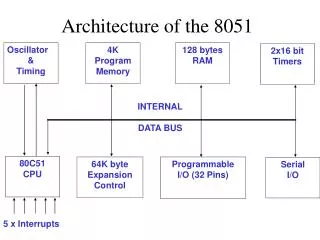
8051 Resources Internal Architecture Pins and Signals Delay Incorporation by software Port operation Memory Interfacing. 8051 Hardware Architecture. Block Diagram of 8051 is. Internal interrupts include - timer interrupts - serial port interrupts

E N D
8051 Resources • Internal Architecture • Pins and Signals • Delay Incorporation by software • Port operation • Memory Interfacing 8051 Hardware Architecture
Internal interrupts include - timer interrupts - serial port interrupts Timer Interrupts – Timer 0 or Timer 1 overflow Serial Port Interrupts – Completion of Transmission or reception or serial data.
Program memory – Total capacity 64 KB (i) 4 KB internal ROM (0000H – 0FFFH) 60 KB external memory (1000H – FFFFH) EA = 5V i.e. External Address is not there for first 4KB. • 64 KB external memory (0000H – FFFFH) EA = 0V i.e. First 4KB is external to processor chip
Data Memory- • External Data Memory =64KB • Internal Data RAM =128 bytes • Special Function Registers =21 Internal Data RAM- • Register Bank 0 to Register Bank 4 – 32 bytes • Direct Bit Addressing – 16 bytes • General Purpose Data Ram – 80 bytes
Memory location 20 to 2F (16 bytes) -Individual bits may be addressed or may be used as bytes • Bits addressed are –
Special Function Registers Special Function Register in 8051 are -
Some of the SFRS (Total 11) are byte as well bit addressable –
Note: observe the vacant space between SFR’s. These can be used an data RAM locations. Stack Operation Stack operation is explained in
Stack in maintained in internal Data RAM PUSH - Stack pointer is incremented. - Data is stored. POP – Data is taken out from stack. - stack pointer is decremented. • stack starts at lower location and grows to higher location as data is pushed. • In 8086, it is opposite.
Data Pointer(DPTR) – 16 bit register (DPH, DPL) – used for storing 16 bit address. Ports(0-3) • 4 bidirectional I/O ports of 8 bits each • P0 and P2 can be used for external memory address lines. • If no external memory then P0, P2 can be used as normal I/O ports. • Lower order Address lines – on (P0.0 to P0.7)(A0 – A7) • Higher order Address lines – (P2.0 to P2.7) (A8 – A15) • P0 - lines also act as data lines – (D0 to D7) • P1 – Act as normal I/O port. Also used for programming of internal memory of 8751.
Port 3 – (P3) can be used as I/O port • P3 pins have important alternate functions • Serial input and output lines • External timer input line • External Data Memory Read and Write Control Signal • External Interrupt Lines Serial Data Buffer (SBUF) – • Holds data to be transmitted on serial lines • Also holds data received from serial lines Receive Shift Register 8051 Internal Bus SBUF Transmit Shift Register
SBUF is connected to two 8 bit shift registers • For data output SBUF loaded to transmit shift register • For data input Receive Shift Register loaded to SBUF Thus transmit and receive can take place at the same time. FULL Duplex Communication
Control and Status Registers • All SFR’s used for controlling the internal resources. • or SFR’s used for knowing the status of resources - belong to this category IP – Interrupt Priority Register IE – Interrupt Enable Register TMOD – Timer Mode Register TCON – Timer Control Register SCON – Serial Control Register PCON – Power Control Register - Will be described along with the resources.
Chip contains as internal bus connected to - 4 KB ROM - 128 byte internal Data RAM - SFR’s – ACC, B Reg, SP, DPTR, PSW, Status and Control Registers ALU – Connected to two temporary registers TMP1 and TMP2. – ACC connected to TMP2 as one operand is in ACC – PSW connected to ALU for status – For reading and writing to internal data RAM-RAM Address Register Stores the address(MAR) – Data read / written in ACC or Register-acts as (MBR)
- Program Address Register • Stores address of instruction to be read from Internal Program Memory (4KB) or External Program Memory • That’s why it is connected to 4KB ROM and port 0 and port 2 pins • Program counter and PC incrementer are connected to program address register. • PC after incrementing is loaded to program address register for reading next instruction. • Instruction Register and Instruction Decoder are part of Timing and control Block. • For external data memory read/write DPTR is connected to port 0 and port 2 • Data to be Written/Data read is transferred through P0 latch.
Bidirectional Buffer is provided to temporarily store branch address as well as operand address. • Bidirectional Ports P0 to P3 have port driver and port latch • Driver is connected to port pins • Latch is connected to internal bus of microprocessor. • DPTR is interfaced to program address register. • Plays major role in external program memory addressing ( MOVC instruction) and external data memory addressing (MOVX) instruction. • Port P0 lines (P0.0 to P0.7) act both as lower address lines (A0 to A7) as well as data lines (D0 to D7) in time multiplex manner.
Information flow in - Program Address Register PC 1. Instruction Read and Decode. Incrementer a b Port 0 – Port 2 Lines Internal Program Memory External Program Memory Fetched Instruction Port 0 Instruction Register Instruction Decoder
2. Operand Read after 1. a e.g. MOV R1, # data • above is repeated. However data is moved to specified Register or memory location. MOV direct, # data 3. Operand Read after 1. e.g. MOV R1, direct Operand is moved to register or address e.g. Direct Address RAM Address Register MOV direct, direct 4. ADD A, R3 ACC TMP 1 ALU Status ACC TMP 2 PSW , , ALU Result R3
5. MOVX, A, @DPTR DPTR Program Address Register Port 0, Port 2 lines External Data Memory Port 0 Specified Register
Port 0 (AD0 – AD7) – 8 bit bidirectional port pins. • Bit addressable pins • Act as lower 8 lines of address bus as well as data lines in time multiplex manner, for external memory access. • Has open collector output. Thus external pull up register is required. Port 1 – 8 bit bidirectional port pins with internal pull up register. Also has role during programming of 8751. Port 2(A8 – A15)- • 8 bit bidirectional port pins with internal pull ups. • Also acts as higher order address lines (A8 – A15) for external memory access. • Also plays part in the programming of 8751.
Port 3 – • 8 bit bidirectional port pins with internal pull ups. port3 pins have important alternate function – P3.0 - RXD (Serial input) P3.1 - TXD (Serial output) P3.2 - INT0 (External interrupt) P3.3 - INT1 (External interrupt) P3.4 - T0 (Timer 0 external input) P3.5 - T1 (Timer 1 external input) P3.6 - WR (External data memory write strobe) P3.7 - RD (External data memory read strobe)
ALE(output)– is sent when external memory address is present in P0 – P2. It can be used to latch the lower address byte from P0. PSEN(output) – Read control signal for program memory. EA(input) – Conveys to microprocessor whether 4KB ROM is on chip or external. EA = 0 (GND) – External EA = 1 (5V) – Internal RST(input) – Reset signal to reset microprocessor.
VPD, VPP, PROG - are used for programming of EPROM in 8751. XTAL1, XTAL2 – pins for connecting crystal. VSS - Ground VCC – (5v) Power • Original 8051 designed and manufacturered by Intel had frequency range 3.5 – 12 MHZ. • With advancements in microelectronics technology,no. of facilities have been incorporated in addition to basic design. The frequency range has also improved. • 8051 is now being produced by no. of firms. Different versions have different frequency range.
The firms which produce 8051 visions apart form Intel are • Dallas Semiconductor (maxim) -Flash memory version • Atmel Corporations • Philips Corporations (Incorporated A to D and D to A on chip) • Frequency range of 8051 from Atmel Corporation include – - 12 MHz (AT 89C51 – 12 PC) - 16 MHz (AT 89C51 – 16 PC) - 20 MHz (AT 89C51 – 20 PC) The register contents when 8051 in reset. Commercial version Plastic DIP Package
Delay incorporation by software • Original 8051 of Intel had 12 clock period machine cycle. • Using frequency of clock and no. of machine cycles the time taken by any instruction can be determined. Example - clock frequency = 12 MHz - clock period = 1/12 microsecond - Time for 1 machine cycle = 12 x 1/12 = 1 microsecond
ORG 00H m/cycle Time(µ sec) MOV R1, # 30H 1 1 MOV A, # 50H 1 1 INC A 1 1 MOV @R1, A 1 1 SJMP $ 4 4 - Apart from MUL and DIV all instructions take 12 or 24 clock period i.e. 1 or 2 machine cycles. - MUL and DIV take 48 clock period i.e. 4 machine cycles.
INS1 - To incorporate 1 second delay between two instructions INS1 and INS2. DELAY Delay Routine must be executed for 1 second DJNZ Rn, Label - takes 24 clock period i.e. 2m/c cycle. If frequency is 12 MHz, m/c cycle = 1 µ sec Execution time for DJNZ Rn, label = 2 µ sec INS2
Rn can take maximum value of 255 one complete loop of will account for delay of 255 x 2 + 1 = 511 µ sec ≈ 29 µ sec - We may envelop it in another loop. MOV Rn, #0FFH DJNZ Rn, $ MOV Rm, # 0FFH DLY 1 : MOV Rn, # 0FFH DJNZ Rn, $ DJNZ Rm, DLY1 a
a a Now will be executed 255 times ≈ 28 µ sec Total execution time of block = x 255 + ex. time for DJNZ Rm, DLY1 x 255 + ex. time for MOV Rm, # 0FFH x 255 + 2 x 255 + 1 = 511 x 255 + 511 ≈ 512 x 256 ≈ 217 µ sec Now 1 sec = 106 µ sec = 103 x 103 µ sec 103 ≈ 210 (1024) 1 sec = 220 µ sec a
The above block should be executed 220 / 217 = 23 = 8 times. Thus to incorporate 2 sec. Delay - MOV R3, # 08H DLY 2 : MOV R4, # 0FFH DLY 1 : MOV R5, # 0FFH DJNZ R5, $ DJNZ R4, DLY1 DJNZ R3, DLY2
It will be more than 1 sec by few milliseconds that can be ignored. These calculations are for 12MHz clock with 12 clock cycles 8051. The above block may be written as subroutine DELAY. DELAY: MOV R3, # 08H - - - - - - - DJNZ R3, DLY2 RET
To incorporate 5 sec. Delay - ACALL DELAY ACALL DELAY ACALL DELAY ACALL DELAY ACALL DELAY • Any amount of delay may be incorporated using this approach. • You may use direct addressing instead of registers.
DELAY : MOV Direct 1, # 08H| | | | DJNZ Direct1, DLY2 RET - For 1 minute delay can be enveloped in a loop that executes 160 times i.e. 3CH times. x x
8051 Port Operation • The ports P0 to P3 are quasi bidirectional i.e. • On reset the ports are configured as output. • To configure any port line as input i.e. to receive data from outside world, 1 must be written to the pin. Example – To configure line 3 of port 2 as input SETB P2.3 instruction can be used. • To configure the port for input operation 1 should be written to each pin of port.
Thus to configure P0 as input SFR addressed For P0 – 80H P1 – 90H P2 – A0H P3 – B0H MOV A, # 0FFH MOV P0, A Port as output - To toggle pins of a port Pk between 0 and 1. REPET : MOV A, # 00H (k=0,1,2,3) MOV Pk, A ACALL DELAY MOV A, # 0FFH MOV Pk, A SJMP REPET may be used.
We may also toggle by writing 0AAH (10 10 1010) and 055H ( 0101 0101). Note both are complement of other. Port as input- MOV A, # 0FFH MOV R3, # 0FH; counter for 15 bytes to be received MOV Pk, A ; configure as input MOV R0, # 30H BACK : MOV A, Pk ; Receive input MOV @ R0, A ACALL DELAY INC R0 DJNZ R3, BACK
Ports P1, P2, P3 have internal pull up registers in the form of FETS. • Port P0 has no internal pull up register called open drain output. To utilize P0 as input or output external pull up register of 10K Ω must be connected to each pin.
Port P0 is open drain since it has address and data in time multiplex way. • P3 pins are used for alternate functions. If alternate functions are not required then P3 pins may be used for I/O operation like other ports. • P0 – P2 may be used for external data memory or external program memory operation. Otherwise these may be used as normal ports.
Memory Interfacing External Memory- • External Data Memory – up to 64 KB Read Control Signal – RD (P3.7) Write Control Signal – WR(P3.6) • External Program Memory - up to 60 KB (8051, 8751) EA=5V - up to 64 KB (8031) EA=0V Read Control Signal = PSEN
Address is sent to memory through • P0(Lower Address Byte) and P2(Higher Address Byte) Data is sent to/from memory through P0. • P0 acts both as Lower address lines as well as data lines in time multiplexed manner. • When Address is present, content of P0 must be latched , so that it can be used for data. • Microprocessor sends a pulse on ALE when address is present.
High to Low transition of ALE may be used to latch the address on a latch. • The latch can be connected to memory to give lower address byte. • P2 is directly connected to higher address lines of memory.