Download
1 / 71
710 likes | 874 Vues
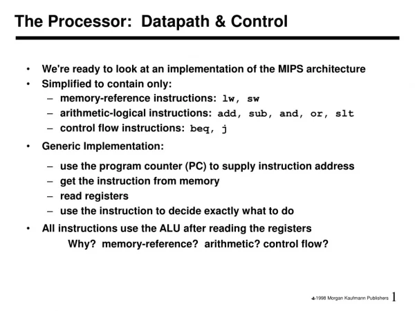
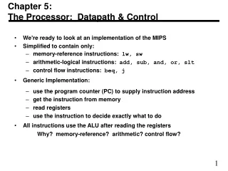
Chapter Five The Processor: Datapath and Control. P. C. S. r. c. M. A. d. d. u. x. A. L. U. A. d. d. 4. r. e. s. u. l. t. S. h. i. f. t. l. e. f. t. 2. R. e. g. i. s. t. e. r. s. A. L. U. o. p. e. r. a. t. i. o. n. 3. R. e. a. d. M. e.

E N D
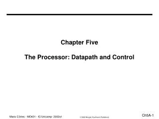
P C S r c M A d d u x A L U A d d 4 r e s u l t S h i f t l e f t 2 R e g i s t e r s A L U o p e r a t i o n 3 R e a d M e m W r i t e A L U S r c R e a d r e g i s t e r 1 P C R e a d a d d r e s s R e a d M e m t o R e g d a t a 1 Z e r o r e g i s t e r 2 I n s t r u c t i o n A L U A L U R e a d W r i t e R e a d A d d r e s s r e s u l t M d a t a r e g i s t e r d a t a 2 M u I n s t r u c t i o n u x W r i t e m e m o r y D a t a x d a t a m e m o r y W r i t e R e g W r i t e d a t a 3 2 1 6 S i g n M e m R e a d e x t e n d Building the Datapath • Use multiplexors to stitch them together
Control • Selecting the operations to perform (ALU, read/write, etc.) • Controlling the flow of data (multiplexor inputs) • Information comes from the 32 bits of the instruction • Example: add $8, $17, $18 Instruction Format: 000000 10001 10010 01000 00000 100000 op rs rt rd shamt funct • ALU's operation based on instruction type and function code
Control • e.g., what should the ALU do with this instruction • Example: lw $1, 100($2) 35 2 1 100 op rs rt 16 bit offset • ALU control input000 AND 001 OR 010 add 110 subtract 111 set-on-less-than • Why is the code for subtract 110 and not 011?
ALU Operation • For load and store instruction, use ALU add to compute memory address. • For R-type instruction, the operation of ALU will be determined by the funct filed, or the lower 6 bits of the 32-bit instruction. • For branch instructions, use ALU subtraction.
ALUOp computed from instruction type Control • Must describe hardware to compute 3-bit ALU control input • given instruction type 00 = lw, sw 01 = beq, 10 = arithmetic • function code for arithmetic • An example of multiple level decoding methodology.
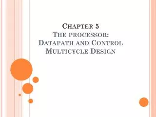
Designing the Main Control Unit • Three instruction classes* : R-type, load or store, branch instruction • Datapath with all necessary multiplexors and all control lines identified: *Limited to the subset of MIPS instructions studied in this chapter.
Control Signals • Seven single-bit control lines, one 2-bit ALUOp control signal • Except for PCSrc, the control signal can be set solely based on the opcode field of the instruction. • To generate PCSrc, we need to AND together a signal from the control unit, which we call Branch, with the Zero signal out of the ALU.
0 M u x A L U A d d 1 r e s u l t A d d R e g D s t 4 B r a n c h M e m R e a d M e m t o R e g I n s t r u c t i o n [ 3 1 2 6 ] C o n t r o l A L U O p M e m W r i t e A L U S r c R e g W r i t e I n s t r u c t i o n [ 2 5 2 1 ] R e a d R e a d r e g i s t e r 1 P C R e a d a d d r e s s d a t a 1 I n s t r u c t i o n [ 2 0 1 6 ] R e a d I n s t r u c t i o n 0 R e g i s t e r s R e a d [ 3 1 0 ] 0 W r i t e M d a t a 2 I n s t r u c t i o n r e g i s t e r u m e m o r y x W r i t e 1 d a t a 0 1 6 3 2 I n s t r u c t i o n [ 1 5 0 ] I n s t r u c t i o n [ 5 0 ] The Simple Datapath with the Control Unit S h i f t l e f t 2 Z e r o r e g i s t e r 2 A L U A L U R e a d A d d r e s s r e s u l t 1 d a t a M M u u I n s t r u c t i o n [ 1 5 1 1 ] x D a t a x 1 m e m o r y W r i t e d a t a S i g n e x t e n d A L U c o n t r o l
Control and Opcode • Will use 6 bit opcodes to set the nine control signals • Figure 5.18 shows the relationship.
Control • Simple combinational logic (truth tables) The ALU control block PLA implementation of the control unit
0 M u x A L U A d d 1 r e s u l t A d d R e g D s t 4 B r a n c h M e m R e a d M e m t o R e g I n s t r u c t i o n [ 3 1 2 6 ] C o n t r o l A L U O p M e m W r i t e A L U S r c R e g W r i t e I n s t r u c t i o n [ 2 5 2 1 ] R e a d R e a d r e g i s t e r 1 P C R e a d a d d r e s s d a t a 1 I n s t r u c t i o n [ 2 0 1 6 ] R e a d I n s t r u c t i o n 0 R e g i s t e r s R e a d [ 3 1 0 ] 0 W r i t e M d a t a 2 I n s t r u c t i o n r e g i s t e r u m e m o r y x W r i t e 1 d a t a 0 1 6 3 2 I n s t r u c t i o n [ 1 5 0 ] I n s t r u c t i o n [ 5 0 ] R-type Instruction Execution Phases • Fetch instruction from memory, increase PC S h i f t l e f t 2 Z e r o r e g i s t e r 2 A L U A L U R e a d A d d r e s s r e s u l t 1 d a t a M M u u I n s t r u c t i o n [ 1 5 1 1 ] x D a t a x 1 m e m o r y W r i t e d a t a S i g n e x t e n d A L U c o n t r o l
0 M u x A L U A d d 1 r e s u l t A d d R e g D s t 4 B r a n c h M e m R e a d M e m t o R e g I n s t r u c t i o n [ 3 1 2 6 ] C o n t r o l A L U O p M e m W r i t e A L U S r c R e g W r i t e I n s t r u c t i o n [ 2 5 2 1 ] R e a d R e a d r e g i s t e r 1 P C R e a d a d d r e s s d a t a 1 I n s t r u c t i o n [ 2 0 1 6 ] R e a I n s t r u c t i o n 0 R e g i s t e r s R e a d [ 3 1 0 ] 0 W r i t e M d a t a 2 I n s t r u c t i o n r e g i s t e r u m e m o r y x W r i t e 1 d a t a 0 1 6 3 2 I n s t r u c t i o n [ 1 5 0 ] I n s t r u c t i o n [ 5 0 ] Phase 2 • Read from two registers S h i f t l e f t 2 d Z e r o r e g i s t e r 2 A L U A L U R e a d A d d r e s s r e s u l t 1 d a t a M M u u I n s t r u c t i o n [ 1 5 1 1 ] x D a t a x 1 m e m o r y W r i t e d a t a S i g n e x t e n d A L U c o n t r o l
0 M u x A L U A d d 1 r e s u l t A d d R e g D s t 4 B r a n c h M e m R e a d M e m t o R e g I n s t r u c t i o n [ 3 1 2 6 ] C o n t r o l A L U O p M e m W r i t e A L U S r c R e g W r i t e I n s t r u c t i o n [ 2 5 2 1 ] R e a d P C R e a d a d d r e s s d a t a 1 I n s t r u c t i o n [ 2 0 1 6 ] I n s t r u c t i o n 0 R e g i s t e r s R e a d [ 3 1 0 ] 0 W r i t e M d a t a 2 I n s t r u c t i o n r e g i s t e r u m e m o r y x W r i t e 1 d a t a 0 1 6 3 2 I n s t r u c t i o n [ 1 5 0 ] A L U c o n t r o l I n s t r u c t i o n [ 5 0 ] Phase 3 • ALU operation S h i f t l e f t 2 R e a d r e g i s t e r 1 R e a d Z e r o r e g i s t e r 2 A L U A L U R e a d A d d r e s s r e s u l t 1 d a t a M M u u I n s t r u c t i o n [ 1 5 1 1 ] x D a t a x 1 m e m o r y W r i t e d a t a S i g n e x t e n d
0 M u x A L U A d d 1 r e s u l t A d d S h i f t l e f t 2 R e g D s t 4 B r a n c h M e m R e a d M e m t o R e g I n s t r u c t i o n [ 3 1 2 6 ] C o n t r o l A L U O p M e m W r i t e A L U S r c R e g W r i t e I n s t r u c t i o n [ 2 5 2 1 ] R e a d P C R e a d a d d r e s s d a t I n s t r u c t i o n [ 2 0 1 6 ] I n s t r u c t i o n 0 R e g i s t e r s [ 3 1 0 ] 0 W r i t e M I n s t r u c t i o n r e g i s t e r u m e m o r y x W r i t e 1 d a t a 0 1 6 3 2 I n s t r u c t i o n [ 1 5 0 ] A L U c o n t r o l I n s t r u c t i o n [ 5 0 ] Phase 4 • Write result to register. R e a d r e g i s t e r 1 a 1 R e a d Z e r o r e g i s t e r 2 A L U R e a d A L U R e a d d a t a 2 A d d r e s s r e s u l t 1 d a t a M M u u I n s t r u c t i o n [ 1 5 1 1 ] x D a t a x 1 m e m o r y W r i t e d a t a S i g n e x t e n d
Our Simple Control Structure • All of the logic is combinational • We wait for everything to settle down, and the right thing to be done • ALU might not produce right answer right away • we use write signals along with clock to determine when to write • Cycle time determined by length of the longest path
M A d d u x 0 4 R e g W r i t e I n s t r u c t i o n [ 2 5 2 1 ] R e a d r e g i s t e r 1 R e a d M e m W r i t e R e a d P C d a t a 1 I n s t r u c t i o n [ 2 0 1 6 ] a d d r e s s R e a d M e m t o R e g A L U S r c r e g i s t e r 2 Z e r o I n s t r u c t i o n R e a d A L U [ 3 1 0 ] R e a d W r i t e d a t a 2 1 A d d r e s s r e s u l t r e g i s t e r d a t a M I n s t r u c t i o n W r i t e u m e m o r y R e g i s t e r s x d a t a D a t a 0 W r i t e m e m o r y R e g D s t d a t a 1 6 3 2 S i g n I n s t r u c t i o n [ 1 5 0 ] e x t e n d M e m R e a d I n s t r u c t i o n [ 5 0 ] A L U O p Performance of Single Cycle Implementation • Calculate cycle time assuming negligible delays except: • memory (200 ps), ALU and adders (100 ps), register file access (50ps) • look at the example in the last part of Sec 5.4 P C S r c 1 A L U A d d r e s u l t S h i f t l e f t 2 1 A L U 1 M M u u I n s t r u c t i o n [ 1 5 1 1 ] x x 0 0 A L U c o n t r o l
Where we are headed • Single Cycle Problems: • what if we had a more complicated instruction like floating point? • wasteful of area • One Solution: • use a smaller cycle time • have different instructions take different numbers of cycles • a multicycle datapath
Multicycle Approach • We will be reusing functional units • ALU used to compute address and to increment PC • Memory used for instruction and data • Introduce new registers in main functional units • IR for storing instruction, MDR for storing data read from memory • A, B registers for storing data read from registers • ALUOut register for storing ALU results • Our control signals will not be determined solely by instruction • We will use a finite state machine for control.
Review: finite state machines • Finite state machines: • a set of states and • next state function (determined by current state and the input) • output function (determined by current state and possibly input) • We’ll use a Moore machine (output based only on current state) N e x t s t a t e N e x t - s t a t e C u r r e n t s t a t e f u n c t i o n C l o c k I n p u t s O u t p u t O u t p u t s f u n c t i o n
Review: finite state machines • Example: • Output: NSLite, EWLite • State: NSGreen, EWGreen • Input: NSCar, EWCar B.10.2: State Diagram
Multicycle Approach • Break up the instructions into steps, each step takes a cycle • balance the amount of work to be done • restrict each cycle to use only one major functional unit • At the end of a cycle • store values for use in later cycles (easiest thing to do) • introduce additional internal registers • Need more multiplexors since we are sharing functional units (ALU, memory). • Justified since cost of registers and multiplexor is much less than ALU or memory.
P C 0 0 I n s t r u c t i o n R e a d M M A [ 2 5 2 1 ] r e g i s t e r 1 u u x x R e a d A I n s t r u c t i o n R e a d Z e r o M e m o r y 1 d a t a 1 1 [ 2 0 1 6 ] r e g i s t e r 2 A L U A L U A L U O u t 0 M e m D a t a R e g i s t e r s r e s u l t I n s t r u c t i o n W r i t e M R e a d [ 1 5 0 ] r e g i s t e r B u 0 d a t a 2 I n s t r u c t i o n W r i t e x [ 1 5 1 1 ] M I n s t r u c t i o n 4 1 W r i t e d a t a 1 u r e g i s t e r d a t a 2 x 0 I n s t r u c t i o n 3 [ 1 5 0 ] M u x M e m o r y 1 1 6 3 2 d a t a S h i f t S i g n r e g i s t e r l e f t 2 e x t e n d MIPS Multicycle Datapath • handling basic instructions d d r e s s
I o r D M e m R e a d M e m W r i t e R e g D s t R e g W r i t e P C 0 I n s t r u c t i o n R e a d M [ 2 5 2 1 ] r e g i s t e r 1 u x R e a d I n s t r u c t i o n R e a d d a t a 1 M e m o r y 1 [ 2 0 1 6 ] r e g i s t e r 2 0 M e m D a t a R e g i s t e r s I n s t r u c t i o n W r i t e R e a d M [ 1 5 0 ] r e g i s t e r d a t a 2 u I n s t r u c t i o n W r i t e x M [ 1 5 1 1 ] I n s t r u c t i o n 4 1 W r i t e d a t a 1 u r e g i s t e r d a t a 0 I n s t r u c t i o n [ 1 5 0 ] M u x 1 1 6 3 2 S h i f t S i g n l e f t 2 e x t e n d I n s t r u c t i o n [ 5 0 ] M e m t o R e g A L U S r c B A L U O p Multicycle Datapath (with control signals) I R W r i t e A L U S r c A 0 M A d d r e s s u x A Z e r o 1 A L U A L U A L U O u t r e s u l t B 0 2 x 3 M e m o r y d a t a A L U r e g i s t e r c o n t r o l
P C W r i t e C o n d P C S o u r c e P C W r i t e A L U O p O u t p u t s I o r D A L U S r c B M e m R e a d A L U S r c A C o n t r o l M e m W r i t e R e g W r i t e M e m t o R e g O p R e g D s t I R W r i t e [ 5 0 ] 0 M u J u m p x I n s t r u c t i a d d r e s s [ 3 1 - 0 ] 2 I n s t r u c t i o n [ 3 1 - 2 6 ] P C 0 I n s t r u c t i o n R e a d M [ 2 5 2 1 ] r e g i s t e r 1 u x R e a d A I n s t r u c t i o n R e a d Z e r o 1 d a t a 1 [ 2 0 1 6 ] r e g i s t e r 2 A L U A L U 0 R e g i s t e r s r e s u l t I n s t r u c t i o n W r i t e M R e a d B [ 1 5 0 ] r e g i s t e r u I n s t r u c t i o n d a t a 2 x [ 1 5 1 1 ] I n s t r u c t i o n 4 W r i t e 1 r e g i s t e r d a t a 0 I n s t r u c t i o n [ 1 5 0 ] M u x M e m o r y 1 1 6 3 2 d a t a A L U S h i f t S i g n r e g i s t e r c o n t r o l l e f t 2 e x t e n d I n s t r u c t i o n [ 5 0 ] Multicycle Datapath (complete) 1 2 6 2 8 o n [ 2 5 0 ] S h i f t l e f t 2 P C [ 3 1 - 2 8 ] 0 M A d d r e s s u x M e m o r y 1 A L U O u t M e m D a t a 0 W r i t e M 1 d a t a u 2 x 3
Five Execution Steps • Instruction Fetch • Instruction Decode and Register Fetch • Execution, Memory Address Computation, or Branch Completion • Memory Access or R-type instruction completion • Write-back step INSTRUCTIONS TAKE FROM 3 - 5 CYCLES!
Role of Control Signals • Refer to Figure 5.29 (p.324) for the action caused by the setting of each control signal. • Pay attention to the actions of 2-bit control signals. (more multiplexors since we are sharing ALUs and memory units in multicycle implementation.)
Step 1: Instruction Fetch • Use PC to get instruction and put it in the Instruction Register. • Increment the PC by 4 and put the result back in the PC. • Can be described succinctly using RTL "Register-Transfer Language" IR <= Memory[PC]; PC <= PC + 4;* Can we figure out the values of the control signals?ForIR = Memory[PC]; Assert MemRead, IRWrite, set IorD to 0 to select PC as the source of the address. For PC <= PC + 4; Set ALUSrcA to 0 (sending PC to ALU), ALUSrcB to 01 (sending 4 to the ALU) and ALUOp to 00 (to make the ALU add), Set PCWrite since we need to write result back to PC. The above two processes occur in parallel. * What is the advantage of updating the PC now?
Step 2: Instruction Decode and Register Fetch • Read registers rs and rt in case we need them • Compute the branch address in case the instruction is a branch • RTL: A <= Reg[IR[25-21]]; B <= Reg[IR[20-16]]; ALUOut <= PC + (sign-extend(IR[15-0]) << 2); • We aren't setting any control lines based on the instruction type (we are busy "decoding" it in our control logic) • Control signal settings:Set ALUSrcA to 0 (so that PC is sent to ALU), ALUSrcB to 11 (so that sign-extended and shifted offset field is sent to ALU), ALUOp to 00 (so ALU adds)
Step 3 (instruction dependent) • ALU is performing one of three functions, based on instruction type • Memory Reference: ALUOut <= A + sign-extend(IR[15-0]); Control signal: Set ALUSrcA to 1 (so that first ALU input is register A), ALUSrcB to 10, ALUOp to 00. • R-type: ALUOut <= A op B;Control signal: Set ALUSrcA to 1, ALUSrcB to 00, ALUOp to 10 (fuct field determines the ALU control signal settings.) • Branch: if (A==B) PC <= ALUOut; Control signal: Set ALUSrcA to 1, ALUSrcB to 00, ALUOp to 01 (subtract). PCCondWrite needs to be asserted to update the PC if Zero output of the ALU is asserted. PCSource set to 01 so that value written into PC will come from ALUOut.
Step 3 (cont’d) • Jump: PC <= PC[31-28] || (IR[25-0]<<2); Control signal: PCWrite asserted, PCSource set to 10
Step 4 (R-type or memory-access) • Loads and stores access memory MDR <= Memory[ALUOut]; or Memory[ALUOut] <= B; Control signal: MemRead asserted (for load), MemWrite asserted (for store), IorD set to 1 (memory address come from ALU) • R-type instructions finish Reg[IR[15-11]] <= ALUOut;Control signal: RegDst set to 1, RegWrite asserted, MemtoReg set to 0.
Step 5 Memory read completion • Reg[IR[20-16]]<= MDR;Control signal: MemtoReg set to 1, RegWrite asserted, RegDst set to 0.
Implementing the Control • Value of control signals is dependent upon: • what instruction is being executed • which step is being performed • Use the information we accumulated to specify a finite state machine • specify the finite state machine graphically, or • use microprogramming • Implementation can be derived from specification • Example (p.330): CPI in a Multicycle CPU using the SPECINT2000 instruction mix shown in Figure 3. 26 (p.228)
S t a r t I n s t r u c t i o n f e t c h / d e c o d e a n d r e g i s t e r f e t c h ( F i g u r e 5 . 3 7 ) M e m o r y a c c e s s R - t y p e i n s t r u c t i o n s B r a n c h i n s t r u c t i o n J u m p i n s t r u c t i o n i n s t r u c t i o n s ( F i g u r e 5 . 3 9 ) ( F i g u r e 5 . 4 0 ) ( F i g u r e 5 . 4 1 ) ( F i g u r e 5 . 3 8 ) High-level View of the FSM Control (Figure 5.32) (Figure 5.33) (Figure 5.34) (Figure 5.35) (Figure 5.36)
FSM for Controlling Memory-Reference Instructions • Has 4 states To state 0 (Fig. 5.32)
FSM for R-Type Instructions • Has 2 states To state 0 (Fig. 5.32)
FSM for Branch Instruction • Single state To state 0 (Fig. 5.32)
FSM for Jump Instruction • Single state To state 0 (Fig. 5.32)
I n s t r u c t i o n d e c o d e / I n s t r u c t i o n f e t c h r e g i s t e r f e t c h M e m R e a d A L U S r c A = 0 I o r D = 0 A L U S r c A = 0 I R W r i t e A L U S r c B = 1 1 A L U S r c B = 0 1 A L U O p = 0 0 A L U O p = 0 0 P C W r i t e P C S o u r c e = 0 0 R = p O ( ) ' W M e m o r y a d d r e s s S ' B r a n c h = J u m p p O c o m p u t a t i o n ( r o E x e c u t i o n c o m p l e t i o n ) c o m p l e t i o n ' W L ' = p O ( A L U S r c A = 1 A L U S r c A = 1 A L U S r c B = 0 0 A L U S r c A = 1 P C W r i t e A L U S r c B = 1 0 A L U O p = 0 1 A L U S r c B = 0 0 P C S o u r c e = 1 0 A L U O p = 0 0 P C W r i t e C o n d A L U O p = 1 0 P C S o u r c e = 0 1 M e m o r y M e m o r y a c c e s s a c c e s s R - t y p e c o m p l e t i o n R e g D s t = 1 M e m R e a d M e m W r i t e R e g W r i t e I o r D = 1 I o r D = 1 M e m t o R e g = 0 W r i t e - b a c k s t e p R e g D s t = 0 R e g W r i t e M e m t o R e g = 1 Graphical Specification of FSM 0 1 • How many state bits will we need? S t a r t ) ' ) e Q ) p ' y t E J - ' B ' = = p p O O ( ( 2 6 8 9 ( ) O ' p W = L ' ' S = W ' ) p O ( 3 5 7 4
CPI in a Multicycle CPU • Compute the CPI given 22% load, 11% store, 49% R-format, 16% branches, 2% jumps.
Finite State Machine for Control • Implementation: a block of combinational logic and a register to hold current state