Download
1 / 35
360 likes | 613 Vues
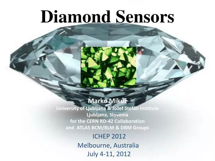
Diamond Sensors. ICHEP 2012 Melbourne, Australia July 4-11 , 20 12. Marko Mikuž University of Ljubljana & Jo žef Stefan Institute Ljubljana, Slovenia for the CERN RD-42 Collaboration a nd ATLAS BCM/BLM & DBM Groups. Outline. Diamond as sensor material RD-42 Diamond suppliers

E N D
Diamond Sensors ICHEP 2012 Melbourne, Australia July 4-11, 2012 Marko Mikuž University of Ljubljana & JožefStefan Institute Ljubljana, Slovenia for the CERN RD-42 Collaboration and ATLAS BCM/BLM & DBM Groups
Outline • Diamond as sensor material • RD-42 • Diamond suppliers • Radiation hardness • Diamond sensor applications - ATLAS • Radiation detection – beam monitors • Beam Conditions Monitor • Beam Loss Monitor • Particle tracking • Diamond Beam Monitor Marko Mikuž: Diamond Sensors
Diamond as Sensor Material Marko Mikuž: Diamond Sensors
Signal from CVD Diamonds • No processing: put electrodes on, apply electric field • Surface preparation and metallization non-trivial ! • Trapping on grain boundaries (pCVD) and in bulk • Much like in heavily irradiated silicon • Parameterized with Charge Collection Distance, defined as • CCD= average distance e-h pairs move apart CCD measured on recent 1.4 mm thick pCVDwafer from E6, and after thinning to 0.8 mm mean not most probable CCDvs. field for pCVD and scCVD diamond Marko Mikuž: Diamond Sensors
Diamond Sensors for HEP: RD-42 K. Andeen17 ,M. Artuso25, F. Bachmair29, L. Bäni29, M. Barbero1, V. Bellini2, V.Belyaev15, E. Berdermann8, P. Bergonzo14, S. Blusk25, A. Borgia25, J-M. Brom10, M. Bruzzi5, M. Cadabeschi19, G. Chiodini32, D. Chren23, V. Cindro12, G. Claus10, M. Cristinziani1, S. Costa2, J. Cumalat24, A. Dabrowski3, R. D’Alessandro6, W. de Boer13, M. Dinardo24, D. Dobos3, W. Dulinski10, V. Eremin9, R. Eusebi30, H. Frais-Kolbl4, A. Furgeri13, C. Gallrapp3, K.K. Gan16, J. Garofoli25, M. Goffe10, J. Goldstein21, A. Golubev11, A. Gorisek12, E. Grigoriev11, J. Grosse-Knetter28, M. Guthoff13, D. Hits17, M. Hoeferkamp26, F. Huegging1, H. Jansen3, J. Janssen1 , H. Kagan16,, R. Kass16, G. Kramberger12, S. Kuleshov11, S. Kwan7, S. Lagomarsino6, A. La Rosa3, A. Lo Giudice18, I. Mandic12, C. Manfredotti18, C. Manfredotti18, A. Martemyanov11, H. Merritt16, M. Mikuz12, M. Mishina7, M. Moench29, J. Moss16, R. Mountain25, S. Mueller13, A. Oh27, P. Olivero18, G. Parrini6, H. Pernegger3, R. Perrino32, M. Pomorski14, R. Potenza2, A. Quadt28, S. Roe3, S. Schnetzer17, T. Schreiner4, S. Sciortino6, S. Seidel26, S. Smith16, B. Sopko23, S. Spagnolo32, S. Spanier31, K. Stenson24, R. Stone17, C. Sutera2, M. Traeger8, W. Trischuk19, D. Tromson14, J-W. Tsung1, C. Tuve2, P. Urquijo25, J. Velthuis21, E. Vittone18, S. Wagner24, R. Wallny29, J.C. Wang25, R. Wang26, P. Weilhammer3,, J. Weingarten28, N. Wermes1 Spokespersons ~100 Participants 1 Universitaet Bonn, Bonn, Germany 2 INFN/University of Catania, Catania, Italy 3 CERN, Geneva, Switzerland 4 FWT Wiener Neustadt, Austria 5 INFN/University of Florence, Florence, Italy 6 Department of Energetics/INFN, Florence, Italy 7 FNAL, Batavia, USA 8 GSI, Darmstadt, Germany 9 Ioffe Institute, St. Petersburg, Russia 10 IPHC, Strasbourg, France 11 ITEP, Moscow, Russia 12 Jozef Stefan Institute, Ljubljana, Slovenia 13 Universitaet Karlsruhe, Karlsruhe, Germany 14 CEA-LIST, Saclay, France 15 MEPHI Institute, Moscow, Russia 16 Ohio State University, Columbus, OH, USA 17 Rutgers University, Piscataway, NJ, USA 18 University of Torino, Torino, Italy 19 University of Toronto, Toronto, ON, Canada 21 University of Bristol, Bristol, UK 23 Czech Technical Univ., Prague, Czech Republic 24 University of Colorado, Boulder, CO, USA 25 Syracuse University, Syracuse, NY, USA 26 University of New Mexico, Albuquerque, NM, USA 27 University of Manchester, Manchester, UK 28 UniversitaetGoettingen, Goettingen, Germany 29 ETH Zurich, Zurich, Switzerland 30 Texas A&M, Collage Park Station, TX USA 31 University of Tennessee, Knoxville TN USA 32 INFN-Lecce, Lecce, Italy 32 Institutes RD42 Collaboration 2012 Marko Mikuž: Diamond Sensors
The Challenge • Sensors for 1st (& 2nd?) tracking layer of experiments at the LHC and more importantly at the HL-LHC • Diamond offers: • Radiation Hardness • Survive to the end of the experiment • Low dielectric constant • Low capacitance → low noise • Low leakage current • Decreases with irradiation • Low readout noise • Room temperature operation • Low mass construction • Fast signal collection • Fluence of interest is O(1016) cm-2 • For 1st pixel layer at R ~4 cm • For R < 25 cm charged particles dominate Pion spectrum at r = 3.7cm Marko Mikuž: Diamond Sensors
Diamond Manufacturers • Many large (~2 cm x 2 cm) sensors delivered in the last year: • Diamond Detectors Ltd, UK • 10 ATLAS Pixel sensors ordered • II-VI Infrared, USA • 4 ATLAS Pixel sensors received • 10 ATLAS Pixel sensors ordered, 10 as option • Now in position to build 30-50 tracking devices ATLAS DBM II-VI DDL 15 cm Marko Mikuž: Diamond Sensors
Radiation Damage Parameterization • Traditionally CCD was fitted with the ansatz • We measure CCD • Radiation-induced traps in fact decrease the mean free path mfp • CCD~mfpe+mfphin thick detectors t >> mfp, CCD • CCD degradation formula not applicable to scCVD since CCD0 = t; mfp0 →∞ • Also for high-quality pCVDCCD0 → t • Relation CCD ↔ mfpfor homogeneous material • For lack of data assume mfpe = mfph • Symmetry of strip CCD to field reversal supportive of the assumption • kmfp robust to mfpe / mfphvariation anyway CCD/t mfpe = mfph mfp = mfpe + mfph mfp/t Marko Mikuž: Diamond Sensors
Irradiation: 24 GeV Protons (PS) • CCD evaluated with strip detectors in CERN test beam • For mean free path expect • With mfp0initial trapping, deduced from CCD0 • kmfp the damage constant • Can turn 1/ mfp0into effective “initial” fluence (x-shifts) • expect mfp0~ ∞ for scCVD • pCVD and scCVD diamond follow the same damage curve • k ~ 0.66x10⁻¹⁸μm-1cm-2 Test beam results with strip detectors Marko Mikuž: Diamond Sensors
Irradiation: 800 MeV Protons (LANL) • Recent irradiations with 800 MeV protons at LANSCE Facility in Los Alamos, US • k ~ 1.2x10⁻¹⁸μm-1cm-2 • ~1.8x more damaging than PS protons • Consistent with NIEL prediction Test beam results Marko Mikuž: Diamond Sensors
Irradiation: 70 MeV Protons (Sendai) • Recent irradiations with 70 MeV protons at Cyric Facility in Sendai, Japan • k ~ 1.7x10⁻¹⁸μm-1cm-2 • ~3x more damaging than PS protons • NIEL prediction • factor of 6 • NIEL violation ?! Test beam results Marko Mikuž: Diamond Sensors
Irradiation: 25 MeV Protons (KIT) • Recent irradiations with 25 MeV protons at Karlsruhe, Germany • k ~ 2.6x10⁻¹⁸μm-1cm-2 • 4x more damaging than PS protons • NIEL prediction • factor of 15 • NIEL violation ! • Work in progress Test beam results Steffen Mueller – PhD Thesis. Marko Mikuž: Diamond Sensors
Diamond Sensor Applications in HEP • All LHC exp’s use diamonds for beam monitoring & accident protection • Current and counting mode operation, TOF capability • O(100) diamond sensors employed • CMS is building Pixel Luminosity Telescope • 48 scCVD pixel modules (5 mm x 5 mm) • ATLAS is building Diamond Beam Monitor • 24 pCVD pixel modules (21 mm x 18 mm) • Upgrade plans include diamond as candidate for innermost pixel tracker layer(s) • Elaborate on ATLAS projects, CMS covered in separate talk • Beam monitoring: ATLAS BCM/BLM • Particle tracking: ATLAS DBM Marko Mikuž: Diamond Sensors
ATLAS BCM/BLM • BCM TOF concept • Collisions: in time • Background: out of time 3.5 m 1.9 m BLM 2 x 6 modules Measured TOF with beam BCM module BLM module 8x8 mm pCVD Marko Mikuž: Diamond Sensors
BLM Beam Dumps – Summer 2011 ~4 orbits Marko Mikuž: Diamond Sensors The LHC beams were dumped twice by BLM due to UFO–like events: 31/07/2011 @ 6:47 and 17/8/2011 @ 9:48 Abort condition: 230 counts on both sides, simultaneous in 2 channels (i.e. 2+2) No aborts this year yet, threshold risen from 230 to 350 due to increased lumi
BLM dump – BCM Post Mortem Info • Single MIP sensitive channels – saturate at ~1k in 5μs bin • 100 MIP sensitive channels – far from saturation. Substantial signal which is ~exponentially increasing beforebeams were extracted (~140/1k).Note: when BLM fired – there was almost no signal in HT BCM channels ~4 orbits saturation beamsdumped ~4 orbits BLM BArequest BLM BArequest beams dumped Marko Mikuž: Diamond Sensors
BCM - BCID Aware Luminosity AND OR XOR-A XOR-C Marko Mikuž: Diamond Sensors
BCM – Preferred ATLAS Lumi Monitor • Robust, stable, (very) low background • Insensitive to pile-up BCM – preferred lumi monitor Marko Mikuž: Diamond Sensors
Diamond Pixel Modules Module after bump bonding Complete module under test • Full modules built with I3 pixel chips @ OSU, IZM and Bonn • Last of those fully built by IZM C-sensor in carrier Pattern with In bumps Edgeless scCVD module pattern scCVD module Bump bonds Marko Mikuž: Diamond Sensors
ATLAS Diamond Beam Monitor • Accepted during last months as add-on to IBL • Contingent on pixel services replacement in 2013 • Spin-off from diamond sensor bid for IBL • 24 diamond pixel modules arranged in 8 telescopes around interaction point provide • Bunch by bunch luminosity monitoring • Bunch by bunch beam spot monitoring • Installation in July 2013 DBM: 3.2<η<3.5 Marko Mikuž: Diamond Sensors
DBM - Installation Pixel DBM BCM BPSS Marko Mikuž: Diamond Sensors
First DBM Modules • First four DBM modules built at IZM last year • 21x18 mm2pCVD from DDL, ~800 μm thick • FE-I4 ATLAS IBL pixel chip • 336x80 = 26880 channels, 50x250 μm2 • Largest ASIC/diamond flip chip assembly • Disassembled, sent to thinning 4 modules after flip-chipping • X-ray perfect • Noise map uniform • Proof of large diamond module assembly • More modules in pipeline now Module on test board Diamond + I4 X-ray after bump bonding I4 only Noise map of a DBM module Marko Mikuž: Diamond Sensors
FE-I4 Tuning with Diamond Christian Gallrapp- CERN Jens Janssen - Bonn Marko Mikuž: Diamond Sensors
DBM Mechanics & Integration • Mechanics & cooling • Getting finalized • Routing of cables from PP0 to PP1 • Agreed • Layout of Type 1 services • Agreed • Follow IBL design for wires • Addressing issues together with Su Dong • PP0 board • Started with layout • Will produce board in the next weeks • System Testing • Produce full on-detector DBM slice: i.e. Module – telescope – PP0 - type 1 services Marko Mikuž: Diamond Sensors
Applications in HEP: wrap-up Beam monitors ATLAS DBM Particle trackers Marko Mikuž: Diamond Sensors
Summary • Recent progress in the diamond world • New promising manufacturers • Improved understanding of radiation damage • Application in all LHC experiments • Building of pixel modules in industry • Diamond trackers under way ! Very interesting times for diamond in HEP ahead of us ! Marko Mikuž: Diamond Sensors
Backup Marko Mikuž: Diamond Sensors
Sensor Types - pCVD • Polycrystalline Chemical Vapour Deposition (pCVD) • Grown in μ-wave reactors on non-diamond substrate • Exist in Φ < 15 cm wafers, >2 mm thick • Small grains merging with growth • Grind off substrate side to improve quality → ~500-700 μm thick detectors Surface view of growth side Photo HK@OSU Side view Test dots on 1 cm grid Photograph courtesy of E6 Marko Mikuž: Diamond Sensors
Sensor Types - scCVD • Single Crystal Chemical Vapour Deposition (scCVD) • Grown on HTHP diamond substrate • Exist in ~ 1 cm2 pieces, max 1.4 cm x 1.4 cm, thickness > 1 mm • A true single crystal • Fall-forward for HL-LHC pixel upgrade (single chips, wafers ?) • Needs significant improvement in size & price, ideas are around • After heavy irradiations properties similar to pCVD, headroom ~3x10¹⁵ p/cm2 • Recent commercial developments in adverse direction • Concentrate on max. ~5x5 mm2 pieces & packaging, main target market: dosimetry • Used on large scale in CMS PLT project ? Marko Mikuž: Diamond Sensors
Manufacturers: Good News • A long lasting strive to identify an alternative supplier to DDL/E6 • II-VI showed promising results ~2 y ago • Order for 10 pcs (option for +10) placed in March with II-VI • Specified CCD > 250 μm at 500 μm thickness • II-VI has grown several thin samples • Very promising CCD • 160 μm on as-grown 400 μm • II-VI seems to know how to grow excellent detector grade diamond • Caveat: to be proven on thick (>1 mm) wafers • Wafer delivered, tested @OSU now Marko Mikuž: Diamond Sensors
Manufacturers: Bad News • DDL has ceased operations • This was a business re-structuring • E6 has agreed to fill order outstanding for ATLAS • Work with E6/DeBeers to remain a strong supplier • Two steps forward, one step back… Marko Mikuž: Diamond Sensors
Radiation Damage in Diamond Charge multiplication • At extreme fluencescharge trapping the paramount radiation damage effect • Difference O(10) in x-section between charged/neutral traps • Filled (neutral) traps trap less (of the opposite carrier) • Basics of “pumping” • Egapin diamond 5 times larger than in Si • Many processes freeze out • Typical emission times order of months • Works also in Si at 300/5 = 60 K – “Lazarus effect” Marko Mikuž: Diamond Sensors
Irradiation at PSI: 300 MeVpions • Single scCVD, d = 500 µm, irradiated with 200 MeVpions at PSI, Villigen, CH • Measured (source) CCD = 260 µm after 6.52x10¹⁴p/cm2 • Turns into mfp of 420 µm • k = 3.6x10⁻¹⁸ µm-1cm-2 • Appears high, but DPA peaks at 200 MeV (Δ) • Again, work in progress • Test-beam under way Steffen Mueller – PhD Thesis. Marko Mikuž: Diamond Sensors
Further DBM Modules • Further 4 diamonds built @ IZM in Feb 12 • ADBM01-4, 500 μm thick • Metallization stand-off “improved” • Uncovered pixels • Irregular pattern • Tested in Bonn, CERN, Gottingen • Limited success • Stable operation up to 500 V on 2 modules • Suspect backplane, PCB • Diamond(s) tested to 1000 V @OSU • Baseline module(s) for April DESY TB, CERN June TB • Metallization moved to OSU • Photolithography • Swap 4 and 5 in module work flow • Steps 3&4 now @ OSU Marko Mikuž: Diamond Sensors
Test-Beam @ CERN • 1st week of June in SPS H6 high energy pion beam • 3 modules as TB candidates • Readout problems • Only SCC148 could be accessed • Module pumped at CERN • Only hitmaps available so far • No obvious dips observable • Track-based analysis needed to confirm CERN Marko Mikuž: Diamond Sensors