Download
1 / 25
310 likes | 692 Vues
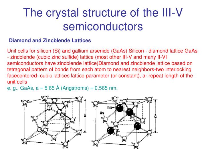
The crystal structure of the III-V semiconductors. Diamond and Zincblende Lattices.

E N D
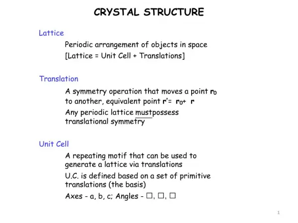
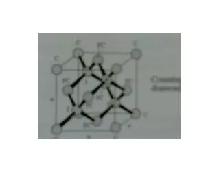
The crystal structure of the III-V semiconductors Diamond and Zincblende Lattices Unit cells for silicon (Si) and gallium arsenide (GaAs) Silicon - diamond lattice GaAs - zincblende (cubic zinc sulfide) lattice (most other III-V and many II-VI semiconductors have zincblende lattice)Diamond and zincblende lattice based on tetragonal pattern of bonds from each atom to nearest neighbors-two interlocking facecentered- cubic lattices lattice parameter (or constant), a- repeat length of the unit cells e. g., GaAs, a = 5.65 Å (Angstroms) = 0.565 nm.
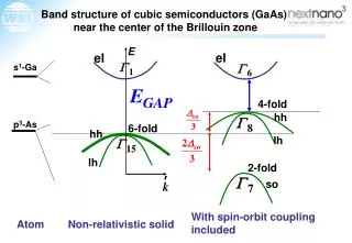
One relevant conduction band is formed from S- like atomic orbitals “unit cell” part of wavefunction is approximately spherically symmetric. The three upper valence bands are formed from (three) P- like orbitals and the spin-orbit interaction splits off lowest, “split-off” hole (i. e., valence) band. The remaining two hole bands have the same energy (“degenerate”) at zone center, but their curvature is different, forming a “heavy hole” (hh) band (broad), and a “light hole” (lh) band (narrower) First Brillouin zone E vs. k banddiagram of zincblende semiconductors
Compound Semiconductors (alloys) For optoelectronics, most devices are fabricated of“compound semiconductors” particularly III-V materials made from •Group III (Al, Ga, In) and •Group V (N, P, As, Sb) elements •Sometimes Si and Ge (Group IV) are used as photodetectors •Sometimes II-VI (e.g. ZnSe) and IV-VI materials (e.g., PbTe) Alloys of compound semiconductors used extensively to adjust the basic materials properties, e.g., lattice constant, bandgap,refractive index, optical emission or detection wavelength EXAMPLE – InxGa1- xAs (where x is the mole fraction of indium) InxGa1- xAs is not strictly crystalline because not every unit cell is identical (random III site location), but we treat such alloys as crystalline to a first approximation
The Human eye response Lasers and LEDs for displays or lighting must emit in the 430-670 nm wavelength region (bandgaps of 3.0-1.9 eV).
Some of the applacations Large Area, Full Color Displays LED Traffic Lights
the first principles calculationguess first compare charge convergence new
Empirical tight binding Hv= < |Hv-ESv|= 0