Download
1 / 32
320 likes | 572 Vues
Introduction to Sensing Probe Microscopy (SPM) Outline. Laboratory safety issues The word of nanotechnology Terminology What is SPM?. Laboratory Safety Review. Laser High Voltages Piezo Scanner Precautions. Laser Safety Information.

E N D
Introduction to Sensing Probe Microscopy (SPM)Outline Laboratory safety issues The word of nanotechnology Terminology What is SPM?
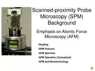
Laboratory Safety Review Laser High Voltages Piezo Scanner Precautions
Laser Safety Information • This system is designed to be used with a class II diode laser with an output of up to 1 mW of visible radiation at 670 nm. • DO NOT stare directly into the laser beam. • WARNING Use of controls or adjustments or performance of procedures other than those specified herein may result in hazardous light exposure. Furthermore, the use of optical instruments with this product may increase eye hazard.
High Voltages • High voltages are present in the instrument. Never open the boxes for servicing or adjustments before disconnecting the AC line cords.
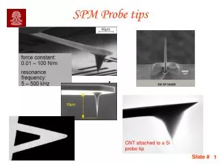
Piezo Scanner Precautions • Piezo scanners are very FRAGILE pieces of equipment. The piezo material that does the scanning is a ceramic and is consequently quite easily broken. Dropping a piezo scanner will result in damage to the scanner that can only be repaired by completely replacing the scanner piezo core. This can be an expensive and time-consuming process and so it is advised that the utmost care is used when handling the scanners. • Agilent Technologies, Inc. recommends that the scanners be stored in the padded scanner case that was supplied with the scanner and that the scanner be kept in a dry environment when not in use. Piezo scanners also perform better with consistent use. If a scanner is not used for some time it may require a short period of use before the scan range is stable and the calibration is correct. It may also be necessary to recalibrate the scanner from time to time.
The world of nanotechnology • http://www.kqed.org/quest/television/fullscreen?id=189 • http://www.nanowerk.com/nanotechnology/videos/Atomic_force_microscopy_at_the_Gerton_Lab.php 2-D and 3-d view of a polymer under studies at SJSU
Scanning Probe Microscopy (SPM)Terminology Atomic Force Microscopy (AFM) • Contact mode • Non contact mode/Acoustic AC Mode (AAC mode) • Phase Imaging • Lateral Force Microscopy (LFM) Scanning Tunneling Microscopy (STM) Magnetic Force Microscopy (MFM) Electric Force Microscopy (EFM) Force Modulation AFM Current Sensing AFM (CSAFM)
What is Scanning Probe Microscopy? … a family of tools for the nanotechnology world..
What is SPM?A Family of Microscopes Scanning Probe Microscopy (SPM)(air, liquid, vacuum) AFM Contact Modes Topography LFM, SThM Lithography Scanning Tunneling Microscopy (STM) Topography Spectroscopy Lithography EChem. BEEM AC Modes Topography MFM, EFM SKPM Others Electro Chemistry
Focusing on Atomic Probe Microscopy Scanning Probe Microscopy • Measuring the current between tip and surface AFM Atomic Force Microscopy • Contact –direct interaction with surface • Non Contact –cantilever vibrates above the surface LFM Lateral Force Microscopy • Forces (frictional) on lateral movement measured MFM Magnetic Force Microscopy • Surface magnetic field imaged And many other techniques….
Scanning Tunneling Microscopy (STM) Measuring the current between tip and surface Requires a conductive surface
Topography Profile Friction Profile Frictional ForceLateral Force Microscopy Low Friction High Friction Low Friction
Lateral Force Microscopy (LFM) Image of Mixed Self-assembled Monolayer in contact mode, in solution )
Vibration Amplitude CantileverVibration Magnetic Domains Magnetic Force Microscopy Magnetic domains on a 5 Gb hard disk: A) Topographic image in close contact mode; B) Phase image after increasing the set point of the same area in A. Both images are 40x40 µm2.
Electrical TestCurrent Sensing AFM Electrical TestI/V Attach electrical test equipment to the probe and make point by point measurements on a surface. Current Voltage
Scratching When Scratching With the AFM, there is a torsion on the cantilever so the probe area changes.
AFM Nanoindenting • The AFM probe is pushed into the sample to cause an indentation • The applied force is calculated from the cantilever mechanics • The AFM sensor measure the probe motion under the applied force • Cantilever stiffness must be matched to the hardness of the sample.
Vibration Amplitude CantileverVibration ++++ Electric field Charged region Electric Force Microscopy
Hierarchy of Measurements Optical Profilometry SEM AFM TEM 10 mm 10 mm 10 nm varying length scale
SEM Comparison SEM - Good Depth of field - Fast scanning • 2D magnification • Need ultra vacuum • Surface has to conduct AFM • Limited depth of field • Contrast on Flat Samples - 3D Magnification • Works in vacuum, ambient air and in liquids
Interaction between Tip and Sample • Scanning a sharp tip mounted on a cantilever across an object surface • Measuring the forces between tip and surface
Potential Diagram Repulsive Cantilever pushed up Distance Potential AttractiveCantilever pulled down
Continuous - Contact Contact Point Potential Distance
Vibrating Mode Potential Distance • The tip is vibrated in and out of the potential associated with the surface.- Large or small amplitudes- Advantages are: low forces, reduced lateral forces
SPM Applications • Life Sciences • Cells, Bio-molecules, Biomaterials • Material Sciences • Semiconductors, Ceramics, Polymers • High Technology • Data Storage, Optics, Semiconductors, Biotech. • Low Technology • Paper, Steel, Plastics, Automobile