Download
1 / 49
490 likes | 531 Vues
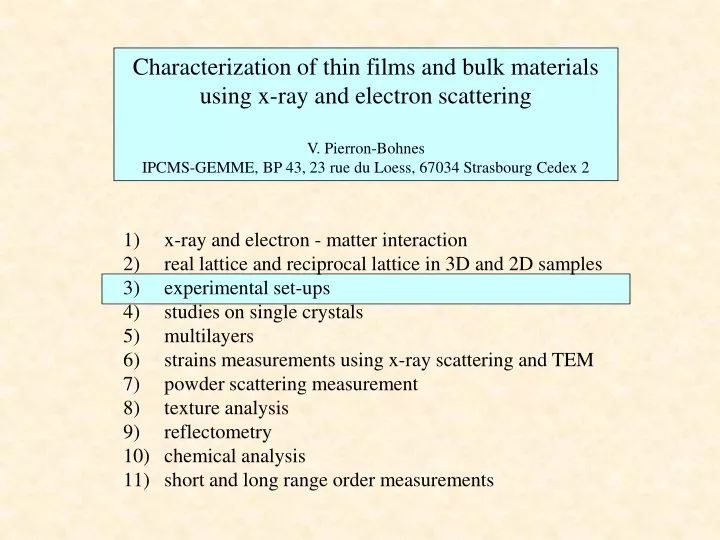
Characterization of thin films and bulk materials using x-ray and electron scattering V. Pierron-Bohnes IPCMS-GEMME, BP 43, 23 rue du Loess, 67034 Strasbourg Cedex 2. Plan : lattices. x-ray and electron - matter interaction real lattice and reciprocal lattice in 3D and 2D samples

E N D
Characterization of thin films and bulk materials using x-ray and electron scattering V. Pierron-Bohnes IPCMS-GEMME, BP 43, 23 rue du Loess, 67034 Strasbourg Cedex 2 Plan : lattices • x-ray and electron - matter interaction • real lattice and reciprocal lattice in 3D and 2D samples • experimental set-ups • studies on single crystals • multilayers • strains measurements using x-ray scattering and TEM • powder scattering measurement • texture analysis • reflectometry • chemical analysis • short and long range order measurements
Diffractometer (x-rays) 2 primary beam monochromator 4 secondary beam monochromator 2q 1 primary source 3 goniometer sample holder 5 detector 2+3 or 3+4: 2 axes diffractometer 2+3+4: 3 axes diffractometer
2 primary beam monochromator 4 secondary beam monochromator 2q 1 primary source 3 goniometer sample holder Diffractometer (x-rays) 5 detector x-rays filament cathode high voltage cable vacuum 1 Primary sources: brilliance (Cu-Ka) electric power Sealed tubes 1010 counts/s 2-3kW Rotating anodes 1011 counts/s 18-25kW Synchrotron 1018 counts/s (ESRF) - glass or ceramics electrons
2 primary beam monochromator 4 secondary beam monochromator 2q 1 primary source 3 goniometer sample holder Diffractometer (x-rays) 2 primary beam monochromators Soller slits highest flux, limits beam divergence Gobel mirror high flux, monochromatic // beam, div.0.02° 1 bent crystal powder diffraction, monochromatic 2 flat crystals monochromatic, exit in line with incidence 4 crystals (Bartels) highest resolution (l) + very // beam (0.0014°)
Diffractometer (x-rays) 2 primary beam monochromator 4 secondary beam monochromator 2q 1 source 3 goniometer sample holder 5 detector 1 Si 4 Ge(220) 12”=0.0033° I/3 2 primary beam monochromators Soller slits highest flux, limits beam divergence Gobel mirror high flux, monochromatic // beam 1 bent crystal powder diffraction, monochromatic 2 flat crystals monochromatic, exit in line with incidence, 4 crystals (Bartels) highest resolution (l) + very // beam (0.0014°) 4 Ge(440) 5”=0.0014° I/75
Diffractometer (x-rays) 2 primary beam monochromator 4 secondary beam monochromator 2q 1 source 3 goniometer sample holder 5 detector j cradle c c 3 goniometer + sample holder 1 rotation w powders 3 rotations w, j, c single crystals, (4-5 axes diffr.) epitaxied layers sample holder support detector support
Diffractometer (x-rays) 2 primary beam monochromator 4 secondary beam monochromator 2q 1 source 3 goniometer sample holder 5 detector 4 secondary beam monochromator Slits + anti-scatter slits highest flux, bad angular resolution Soller slits high flux, angular resolution 0.1-0.4° Gobel mirror high flux, no fluor., good angular resol. high speed investigation of rec. space 2 flat crystals best resolution in angle and energy (l)
Diffractometer (x-rays) 2 primary beam monochromator 4 secondary beam monochromator 2q 1 source 3 goniometer sample holder 5 detector 5 detector proportional counters (gaz ionisation), microchanel plates (photomultiplicator), semiconductor detectors (e--hole pair formation), scintillators (light emission) punctual (1cmx1cm), linear (10cmx1cm), curved (120°), CCD plates curved detector monochromator tube sample
x-rays O A crystal in a diffractometer, what happens ? no diffraction : l 0.1 nm incident Ewald circle: radius 2p/l reciprocal lattice of the crystal transmitted
O diffraction of the wave Bragg law incident diffracted 2q transmitted
O multicounters :w fixed + 2q varies rapid measurements on powders mapping of the reciprocal space scan geometries1 w sample surface varies direction varies direction fixed in the reciprocal space 2q
O Rocking curves : 2q fixed + w varies optimization of the orientation of the specimen coherence length Q study of textures… scan geometries2 w sample surface fixed direction varies in the reciprocal space 2q
O w/2q :q – w = q + e = a= Cste; q,wvary together lattice parameter measurement coherence length // Q mapping the reciprocal space scan geometries3 w sample surface sample normal a Dw = dq p/2+q-w = cste p/2+q-w p/2-q e direction fixed 2q
O q/2q :q = w = e vary together lattice parameter surface for epitaxied films study of planes // surface coherence length surface structure of powders scan geometries4 w sample surface p/2-q surface e 2q
q/2q :q = w = e = p/2 maximum Q Q = 4p/l scan geometries5 sample surface w e surface O 2q
Limitations in the reciprocal space in reflection : w > 0 ; e > 0 scan geometries6 sample surface w = 0 O e = 0
Example: L10 CoPt j z-variant z x fundamental peaks superstructure peaks: x-variant superstructure peaks: z-variant sample position superstructure peaks: y-variant
j Example: L10 CoPt
alignment of a diffractometer1) the incident beam is // plate2) the beam crosses the plate center3) origin of 2q in the incident beam4) specimen center on plate center5) j rotation within specimen surface I0 I0/2 w rotation center
Resolution in x-ray diffraction wavelength spread analyzor Ge(440) mono- chromator Ge(440) range in the reciprocal space where the intensity is integrated due to the entry and exit slits
Electron diffraction LEED (low energy electron diffraction) energy = 20 - 200 eV → crystal surface grids fluorescent screen Omicron
Electron diffraction: RHEED (Reflection High Energy Electron Diffraction) Scheme of RHEED diffraction. fluorescent screen shadow electrons sample Construction of the diffraction conditions with the Ewald sphere. RHEED intensity oscillations (01) spot measured during the growth of a GaAs(100)-(2x4) surface at E = 12.5 keV with k0//[110]. RHEED image of CoPt deposited by MBE full planes half full planes
Electron diffraction: TEM (Transmission Electron Microscope) 1000kV 120kV 2m 2m
Transmission Electron Microscope EDX EELS TEM
wavelength • ≈ 0.001 nm : fine for crystallography ! E (eV)
Sources Richardson law: i = AT2 exp(-F/kT) metal | vacuum
Column difficult optic many aberrations Resolution >>
Electron diffraction in TEM incident : l 0.001 nm Ewald sphere O
Laue zones Experimental pattern on gold <001>
Example : CoPt/Pt/MgO prepared at 680K Diffraction in plane-view e- http://temsamprep.in2p3.fr [110](001)//[110](001) → 3 growth directions z-variant z x O. Ersen Thesis, Strasbourg, 2002
Example : CoPt/Pt/MgO diffraction [110](001)//[110](001) [1-10](111)//[110](001) [-1-12](111)//[110](001) prepared at 680K Diffraction in plane-view e- → 3 growth directions z-variant z x O. Ersen Thesis, Strasbourg, 2002
Dark field image showing the different grains in CoPt/Pt/MgO Grains b+d O. Ersen Thesis, Strasbourg, 2002
Dark field image showing the different grains in CoPt/Pt/MgO Grains b order O. Ersen Thesis, Strasbourg, 2002
Dark field image showing the different grains in CoPt/Pt/MgO Grains d O. Ersen Thesis, Strasbourg, 2002
Dark field image showing the different grains in CoPt/Pt/MgO Grains c O. Ersen Thesis, Strasbourg, 2002
conventional image [Co 6 nm/Mn 0.4 nm]12
B C A [Co 6 nm/Mn 0.4 nm]12 diffraction ABCABC… ACBACB… ABAB… 00.4 222 222twin - - - [111]fcc [0001]hcp Co+Mn Ru A. Michel, Thesis, Strasbourg, 1995
[Co 6 nm/Mn 0.4 nm]12 epitaxied on Ru TEM and X-ray diffraction Co hcp Ru hcp Co fcc Co hcp Ru hcp Co fcc twinned A. Michel et al, Eur. Phys. J. B 19 225 (2001).
internal standard [Co 6 nm/Mn 0.4 nm]12 epitaxied on Ru Co hcp Ru hcp radius R d(2q) = dz sin2q/Rsinw Co fcc w Co hcp / / / / / / / / / / Ru hcp dz dz sin2q/sinw dz/sinw Co fcc twinned 2q sample surface
Contrasts in TEMBright field with transmitted beam contrast : defects (strains) + absorption dislocations precipitates
Chemical analysis: concentration values and profiles Example : precipitates at grain boundaries + inside the grains (different sizes)
high resolution Cu-rich plane Guinier-Preston zones In Al-Cu4% HRTEM along [001]
high resolution: ordered CoPt cross section O. Ersen Thesis, Strasbourg, 2002 A B
high resolution: ordered CoPt cross section A O. Ersen Thesis, Strasbourg, 2002 fringes ordered phase ? Dislocation in MnPt (Borme, thesis, Grenoble 2006) B interface regular black and white contrasts epitaxial strains
high resolution: image simulations O. Ersen Thesis, Strasbourg, 2002 15.2nm HRTEM images simulated using the EMS programme for a CoPt disordered fcc phase, along [100]. The objective defocalization varies with -10 nm steps. The thickness step (1.9 nm) corresponds to 5 elementary cells. specimen thickness 1.9nm 0 –70 objective defocalization
high resolution: image simulations O. Ersen Thesis, Strasbourg, 2002 15.2nm HRTEM images simulated using the EMS programme for a CoPt L10 ordered phase (z-variant), along [100]. The objective defocalization varies with -10 nm steps. The thickness step (1.9 nm) corresponds to 5 elementary cells. specimen thickness 1.9nm 0 –70 objective defocalization
high resolution: image simulations O. Ersen Thesis, Strasbourg, 2002 disordered HRTEM images simulated using the EMS programme for a mixing of L10 ordered and disordered CoPt phases (z-variant), along [100]. The objective defocalization varies with -10 nm steps. The proportion step is 14.5%. disordered phase proportion ordered 0 –70 objective defocalization
GaAs observed along [110] Defocalization: -60nm to -140nm Specimen thickness: 11nm to 27 nm http://www.cemes.fr/microscopie/haute res.htm
Digitally processed images from the sample [Co 6 nm/Mn 0.4 nm]12 Mn Inverse FT using the [1011]hcp HRTEM image Inverse FT using the [111]fcc Inverse FT using the [111]fcc-t A. Michel et al, Eur. Phys. J. B 19 225 (2001).