Download
1 / 22
320 likes | 677 Vues
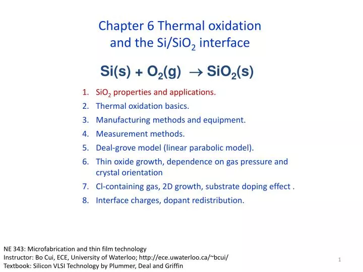
Chapter 6 Thermal oxidation and the Si/SiO 2 interface. Si(s) + O 2 (g) SiO 2 (s). SiO 2 properties and applications. Thermal oxidation basics. Manufacturing methods and equipment. Measurement methods. Deal-grove model (linear parabolic model).

E N D
Chapter 6 Thermal oxidation and the Si/SiO2 interface Si(s) + O2(g) SiO2(s) SiO2 properties and applications. Thermal oxidation basics. Manufacturing methods and equipment. Measurement methods. Deal-grove model (linear parabolic model). Thin oxide growth, dependence on gas pressure and crystal orientation Cl-containing gas, 2D growth, substrate doping effect . Interface charges, dopant redistribution. NE 343: Microfabrication and thin film technology Instructor: Bo Cui, ECE, University of Waterloo; http://ece.uwaterloo.ca/~bcui/ Textbook: Silicon VLSI Technology by Plummer, Deal and Griffin
Properties of thermally grown SiO2 • Atomic density: 2.31022 molecules/cm3 • (For Si, it is 51022 atoms/cm3) • Refractive index: n=1.46 • Dielectric constant: =3.9 (why not =n2?) • Excellent electrical insulator: resistivity > 1020cm, energy gap Eg=8-9 eV. • High breakdown electric field: >107 V/cm • It is amorphous. • Stable, reproducible and conformal SiO2 growth • Melting point: 1700C • Density: 2.21 g/cm3 (almost the same as Si that is 2.33 g/cm3) • Crystalline SiO2 [Quartz] = 2.65gm/cm3 Conformal growth
The Si/SiO2 interface Thermal oxide (amorphous) Si substrate (single crystal) The perfect interface between Si and SiO2 is one major reason why Si is used for semiconductor devices (instead of Ge…)
Application of SiO2 in IC industry STI STI: shallow trench isolation Very good etching selectivity between Si and SiO2 using HF
Diffusion mask for common dopants SiO2 can provide a selective mask against diffusion at high temperatures. (DSiO2 << Dsi) Oxides used for masking are 0.5-1μm thick. (not good for Ga) Mask thickness (m) Can also be used for mask against ion implantation Diffusion time (hr) SiO2 masks for B and P
Use of oxide in MOSFET Gate oxide, only 0.8nm thick! As insulation material between interconnection levels and adjacent devices LOCOS: local oxidation isolation; STI: shallow trench isolation
Local Oxidation of Si (LOCOS) Fully recessed process attempts to minimize bird’s peak.
For nanofabrication: oxidation sharpening for sharp AFM tips or field emitters for display Si SiO2 Field emission display (FED) Ding, “Silicon Field Emission Arrays With Atomically Sharp Tips: Turn-On Voltage and the Effect of Tip Radius Distribution”, 2002.
桥联氧 非桥联氧 Oxide Structure Bridging oxygen Non-bridging Amorphous tetrahedral network Basic structure of silica: a silicon atom tetrahedrally bonds to four oxygen atoms The structure of silicon-silicon dioxide interface: some silicon atoms have dangling bonds.
Oxide Structure Single crystal (quartz) 2.65 g/cm3 Amouphous (thermal oxide). 2.21 g/cm3
Chapter 6 Thermal oxidation and the Si/SiO2 interface SiO2 properties and applications. Thermal oxidation basics. Manufacturing methods and equipment. Measurement methods. Deal-grove model (linear parabolic model). Thin oxide growth, dependence on gas pressure and crystal orientation Cl-containing gas, 2D growth, substrate doping effect . Interface charges, dopant redistribution. NE 343 Microfabrication and thin film technology Instructor: Bo Cui, ECE, University of Waterloo Textbook: Silicon VLSI Technology by Plummer, Deal and Griffin
Dry and wet oxidation Dry oxidation: Si(s) + O2(g) SiO2(s); Wet/steam oxidation: Si(s) + 2H2O(g) SiO2(s) + 2H2(g) • Both typically 900-1200°C, wet oxidation is about 10 faster than dry oxidation. • Dry oxide: thin 0.05-0.5m, excellent insulator, for gate oxides; for very thin gate oxides, may add nitrogen to form oxynitrides. • Wet oxide: thick <2.5 m, good insulator, for field oxides or masking. Quality suffers due to the diffusion of the hydrogen gas out of the film, which creates paths that electrons can follow. • Room temperature Si in air creates “native oxide”: very thin 1-2nm, poor insulator, but can impede surface processing of Si. • Volume expansion by 2.2 (=1/0.46), so SiO2 film has compressive stress. Xox is final oxide thickness Si wafer = 0.46
Chapter 6 Thermal oxidation and the Si/SiO2 interface SiO2 properties and applications. Thermal oxidation basics. Manufacturing methods and equipment. Measurement methods. Deal-grove model (linear parabolic model). Thin oxide growth, dependence on gas pressure and crystal orientation Cl-containing gas, 2D growth, substrate doping effect . Interface charges, dopant redistribution. NE 343 Microfabrication and thin film technology Instructor: Bo Cui, ECE, University of Waterloo Textbook: Silicon VLSI Technology by Plummer, Deal and Griffin
Thermal silicon oxidation methods A three-tube horizontal furnace with multi-zone temperature control Vertical furnace (not popular) Wet oxidation using H2 and O2 is more popular (cleaner) than using H2O vapor.
Thermal oxidation equipment • The tubular reactor made of quartz or glass, heated by resistance. • Oxygen or water vapor flows through the reactor and past the silicon wafers, with a typical velocity of order 1cm/s.
Thermal oxidation in practice Clean the wafers (RCA clean, very important) Put wafers in the boat Load the wafers in the furnace Ramp up the furnace to process temperature in N2 (prevents oxidation from occurring) Stabilize Process (wet or dry oxidation) Anneal in N2. Again, nitrogen stops oxidation process. Ramp down
Chapter 6 Thermal oxidation and the Si/SiO2 interface SiO2 properties and applications. Thermal oxidation basics. Manufacturing methods and equipment. Measurement methods (mechanical, optical, electrical). Deal-grove model (linear parabolic model). Thin oxide growth, dependence on gas pressure and crystal orientation Cl-containing gas, 2D growth, substrate doping effect . Interface charges, dopant redistribution. NE 343 Microfabrication and thin film technology Instructor: Bo Cui, ECE, University of Waterloo Textbook: Silicon VLSI Technology by Plummer, Deal and Griffin
Stylus Surface profilometry (Dektak): mechanical thickness measurement Oxide etched away by HF over part of the wafer and a mechanical stylus is dragged over the resulting step. Mirror image of stylus stylus AFM can also be used for thickness measurement. (AFM: atomic force microscopy)
Thickness determination by looking the color Relative illumination intensity Film thickness (nm) • Oxide thickness for constructive interference (viewed from above =0o) Xo=k/2n, n=1.46, k=1, 2, 3… • Our eye can tell the color difference between two films having 10nm thickness difference.
Optical thickness measurement: ellipsometry Very accurate (1nm accuracy) • After quarter wave plate, the linear polarized light becomes circular polarized, which is incident on the oxide covered wafer. • The polarization of the reflected light, which depends on the thickness and refractive index (usually known) of the oxide layer, is determined and used to calculate the oxide thickness. • Multiple wavelengths/incident angles can be used to measure thickness/refractive index of each film in a multi-film stack.
Electrical thickness measurement: C-V of MOSFET Small AC voltage is applied on top of the DC voltage for capacitance measurement. Substrate is N-type. Electron is majority carrier, hole is minority carrier. Accumulation: positive gate voltage attracts electrons to the interface. Depletion: negative gate bias pushes electrons away from interface. No charge at interface. Two capacitance in series. Inversion: further increase (negative) gate voltage causes holes to appear at the interface.
Effect of frequency for AC capacitance measurement At/after inversion: For low frequency, (minority) charge generation at the interface can follow the AC field to balance the charge at the gate, so Cinv=Cox. For high frequency, the gate charge has to be balanced by the carrier deep below the interface, so Cinv-1 = Cox-1 + CSi-1. Deep depletion: for high scanning speed (the DC voltage scan fast into large positive voltage), depletion depth Xd must increase to balance the gate charge. P-type substrate here (previous slide N-type) • Parameter from C-V measurement: • Dielectric constant of Si & SiO2 • Capacitor area • Oxide thickness • Impurity profile in Si • Threshold voltage of MOS capacitor