Download
1 / 5
50 likes | 243 Vues
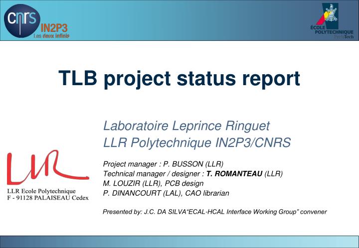
TLB project status report. Laboratoire Leprince Ringuet LLR Polytechnique IN2P3/CNRS Project manager : P. BUSSON (LLR) Technical manager / designer : T. ROMANTEAU (LLR) M. LOUZIR (LLR), PCB design P. DINANCOURT (LAL), CAO librarian

E N D
TLB project status report LaboratoireLeprinceRinguet LLR Polytechnique IN2P3/CNRS Project manager : P. BUSSON (LLR) Technical manager / designer : T. ROMANTEAU (LLR) M. LOUZIR (LLR), PCB design P. DINANCOURT (LAL), CAO librarian Presented by: J.C. DA SILVA“ECAL-HCAL Interface Working Group” convener
Project goalsTLB purpose and requirements “Test Link Board” (TLB), a design study platform for modern serial link • Set up of a CAD design flow for Multi Giga Transceiver (MGT) • Importance of simulations for 4 Gbpsto 10 Gbps links • High number of parameters (CTLE, DFE, FFE), optimization needed • Analogue and digital effects modeling in IBIS-AMI models • Design methodology for advanced Signal Integrity (SI) PCB • Allegro constraints manager (Cadence) design basis for PCB routing • Applicable for CMS’s TCCxx upgrade • No software change at a first step : TLB must be plugged on TCCxx cards (SLB like) • Useful for TCCxx/oSLBtest bench development Studies for trigger implementation and TCCxx/oSLBtest bench • 4,8 Gbps base line with a more compact data format for TCCxx upgrade • Use as SLB like, up to 23 bits free in frame can now be used for “real time bunch tag” • For E-Endcap 9 bits trigger vector can be upgraded to 11 bits • TCCxx/oSLBtest bench development in charge at LLR • Optical I/O available, take profit as real time survey • Auto align algorithm between TBL card • Spy buffer for TTC command history • Predictable pattern generator for data checking at test bench receiver side J. Da Silva ECAL-HCAL IWG
Architecture for TLBConstraints / Hardware choices Mechanic constraints • TLB must be plugged on a TCC48 card : • used in a 1 slot VMEwidth → low profile components on bottom side of TLB • SFP+ not compatible with TCCxx → TLB’s PCB is extended outside the front pannel of TCCxx cards • Low space available on PCB, three high density connectors for TCCxx plugging • Up to 9 TLB could be plugged on TCC68/TCC48 mother board Electronic constraints, solutions and associated technologies • 4,8 Gbps min → 1 FPGA XCVLX6 with 8 GTX MGT serdes (6,6 Gbps max, 2 used) • 3,3V level signal on TCCxx side, 2,5V on TLB → buffered level translator • Very low clock jitter for clock of MGT → clock jitter reduction device is used • Mono 3,3V power supply source, low noise power supply requested for MGT • Low chip count requested → 2 x LTM4615 devices with low mechanical profile : 2 x DC/DC converters + 1 x LVDO linear regulator per device Architecture choices • Embed two SFP+ optical transceiver as available reference solution • One alone, firmware downloaded from a low cost EEPROM solution from Xilinx • JTAG hardware and software reused from TCC48 platform J. Da Silva ECAL-HCAL IWG
Design methods automation Status of the design CAO based design • New PCB and schematic symbols were developed at LAL Orsay and LLR • Pre layout simulation performed on critical nets to define constraint templates • PCB routing based on constraints previously simulated and/or entering • Clock jitter reduction solution tested on a separate testing platform then implemented Firmware code development • Version “SLB like” purpose, code writing is greatly advanced but not complete • Full VHDL description, attempt to be DO-254 compliant TLB design status (Design started at end of February 2011) • Schematic complete, few update added in accordance with VHDL code development • Signal integrity simulation is in progress • PCB technology and cross section largely discussed with manufacturer • Via in Pad solution adopted to solve implementation of complex power supply system in a low space • Laser via and blind via adopted to solve the high net density and low pin spacing • Class 7, PCB design at LLR not fully completed • Available on Q1-2012 J. Da Silva ECAL-HCAL IWG
PCB routing highlightPower supply detailed view / global view TLB → SLB elongated mechanical format • Power supply system on bottom side (low profile) • JTAG EPROM on bottom side • All others components on top side • High density “SLB like” connector • Level translator buffer • FPGA • Clock jitter cleaner • Small from factor card cage (SFP+) Power supply based on 2 x LM4615 • Via in all pad of LM4615 • External filtering components • Low noise MGT supply included • 2 internal layer power plan • Complex power scheme • 3.3V, 2,5V, 1.8V, 1.5V, 1V-VCCINT • 1,2V-MGT, 1V-MGT J. Da Silva ECAL-HCAL IWG