Download
1 / 10
100 likes | 177 Vues
QIE10 Issues. Tom Zimmerman Fermilab Oct. 28, 2009. (noise, …). (statistics). (errors, non-uniformities). Uniform ADC quantization error (increasing precision at higher energies). OK, but inefficient !. This precision is sufficient! (Constant precision at higher energies )

E N D
QIE10 Issues Tom Zimmerman Fermilab Oct. 28, 2009
(noise, …) (statistics) (errors, non-uniformities) Uniform ADC quantization error (increasing precision at higher energies). OK, but inefficient! This precision is sufficient! (Constantprecision at higher energies) Floating point result: Exponent + Mantissa The generic problem:digitizing photodetector charge pulses 1) over wide dynamic range (typically 13-18 bits) 2) with negligible quantization error 3) at high rate (typically around 50 MHz) Constant precision implies that ADC bin width is not uniform, but proportional to energy.
A time-tested solution: QIE • QIE = Charge Integrator and Encoder. • Digitizes wide dynamic range signals in a floating point format • Older versions of QIE required an off-chip commercial ADC • Newer versions incorporate an on-chip ADC: single-chip solution • Integrate input charge on multiple scaled ranges simultaneously • Select one appropriate range for any given input amplitude • Digitize the integrator output on that range • Read out the digitized result (mantissa) and the range code (exponent) • Pipeline all operations to obtain deadtimeless acquisition and readout • Scaling ratios between ranges must be constant to allow slope/offset calibration • Controlled input impedance over wide dynamic range Some advantages of the QIE approach Single-chip solution is straightforward with few external components: high channel density. Efficient floating point on-chip ADC minimizes power and data going off the detector.
Range Code • 5) The range code forms the exponent. • 4) For a given input charge, one appropriate range output is selected and digitized by an ADC, forming the mantissa. • 3) Splitter ratios and integration C ratios are chosen to achieve range-to-range scaling of the transfer gain (I/C) by factor A. • 2) Each splitter range output feeds a charge integrator. The current fractions are integrated simultaneously on all ranges. • 1) Input current pulses are divided into weighted fractions by a current splitter The QIE Concept (simplified)
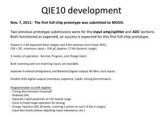
QIE10 for CMS • Least count charge (LSB) = 3 fC • Max. input charge = 330 pC (~17-bit range) • Dual polarity input desired: • Negative input current from PMT through coaxial cable: • need constant impedance (50 ohm) input over wide range (sub-uA to 60 mA): not trivial! • Positive input current from SiPM or APD (short cable): • need low impedance (~ 10 ohm) input • Multi-range system to accommodate wide dynamic range: • Propose 4 QIE ranges, each scaled by factor of 8 • ADC has 4 “segments” per QIE range: bin widths 1, 2, 4, 8 to maintain “constant” resolution • Input impedance (negative input) should look resistive to high freq. (1GHz) to minimize reflections • Constant resolution level of better than 2% • Deadtimeless operation: integrate all input charge every 25 ns, read out at 40 MHz • Fast analog signal bandwidth (100MHz) • TDC – new feature not previously implemented on any QIE chips • Clock phase adjust – new feature not previously implemented on any QIE chips
QIE10: what process to use? Input splitter must have constant split ratios over wide range: not possible with MOS. Need bipolars!! Bipolar NPNs are also instrumental in obtaining a controlled impedance input. CMOS required for switches, logic. This design configuration requires a BiCMOS process Voltage requirements “Stacked configuration”: Splitter 2V Current switches 1V Integrators 1V Headroom 1V This design configuration requires a 5V process Earlier versions of QIE: AMS 0.8u BiCMOS process. This is an older process -- still available, but only for dedicated runs, not multi-project prototyping runs through silicon brokers (like MOSIS). AMS 0.35u SiGeBiCMOSis a more modern process, available for multi-project runs through MOSIS. This is a 3.3V process, but has optional 5V NPN and CMOS transistors available. Start using it!
Proposed negative input circuit for CMS QIE10 range-to range Scaling Factor = 8 C 2C 8C 32C Input current splitter 2 I I/4 I/8 I/16 X16 X4 X2 X1 gm3 gm1 1 VDC bondpad bondpad DC bias (Ref. voltage generated Internally) CEXT 0.5u REXT1 19 Small signal: Feedback circuit gm2 Must avoid turning on protection diodes (Rin =< 20 ohms) 20 ohms bondpad REXT2 30 (feedback active, set Rin = 20 ohms) • Nice properties of this BiCMOS circuit: • Small bipolar transistors give good gm, good speed (>100 MHz). • Split ratios are constant over wide range with a bipolar splitter • As Iin increases, gm1 increases but gm3 decreases, • so that Rin ~ constant! Arrange VDC for Rin = 20. • Rin looks resistive to > 1GHz! Large signal: 50 ohms Rin ~ 20 ohms (feedback circuit inactive) Iin (peak ~60 mA)
Proposed positive input circuit for CMS QIE10 (Invert and split the signal current) Iin DC bias bondpad Low input R <= 12 ohms I I/4 I/8 I/16 X23 X16 X4 X2 X1 Identical to negative input splitter Feedback amp for low input R NPN current mirror gives signal inversion, good linearity
Proposed QIE10 on-chip Flash ADC characteristics: 6 bits (64 bins of varying width). Input charge (fC)effective ADC bin size (fC) 0 – 50 3 50 – 160 6 160 – 400 12 400 – 900 24 900 – 1900 48 1900 – 1600 96 4K – 8K 192 8K – 16K 384 16K – 32K 768 32K – 64K 1.5K 64K – 128K 3K 128K – 256K 6K 256K – 330K 12K The ADC digitizes only one of the 4 ranges for a given input charge. 4 ADC segments per QIE range Range 0 Range 1 (X8) Range 2 (X64) ADC resolution stays constant within a factor of 2. Worst case resolution = 1.4%. Range 3 (X512) This FADC is “non-linear” in the sense that it has non-uniform bin widths. However, it’s really a linear FADC with “missing” comparators, strategically “removed” since they are not necessary. Improves speed, area, power, etc. This 64-bin ADC has the same range as a 192-bin (7.5 bit) “linear” ADC (where all bins are of equal width).
First planned test chip submission Design work completed to date (simulation only): Negative input amp/splitter Positive input amp/splitter Current switches Integrators Starting schematic entry and layout 10/09 Objectives: Gain experience with 0.35u process -- confirm simulation accuracy -- NPN splitter matching, linearity Radiation testing? (SiGe supposed to be more rad hard) If this prototype works as expected, continue to full-chip design and layout. 4-phase Integrator Cint 4-phase Integrator 2Cint 4-phase Integrator 8Cint 4-phase Integrator 32Cint 4-way Current Switch 4-way Current Switch 4-way Current Switch 4-way Current Switch Negative Input Amp/splitter Positive Input Amp/splitter