Download
1 / 28
280 likes | 291 Vues
This project focuses on the design of front-end modules for the ATLAS Strips Detector at the SLHC, including cooling, data and DCs fibers, interlocks, and more.

E N D
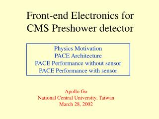
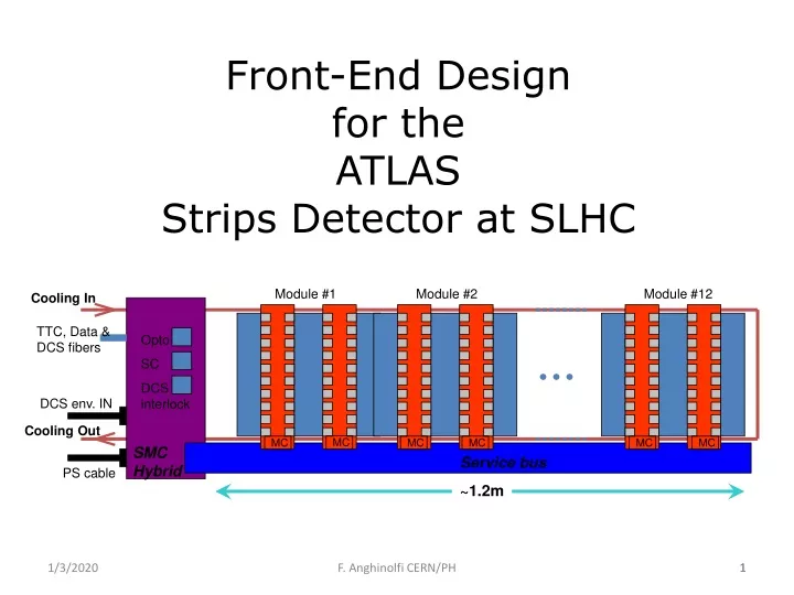
Front-End Design for the ATLASStrips Detector at SLHC Module #1 Module #2 Module #12 Cooling In TTC, Data & DCS fibers Opto SC DCS interlock DCS env. IN Cooling Out SMC Hybrid Service bus PS cable ~1.2m MC MC MC MC MC MC F. Anghinolfi CERN/PH 1
ABCN in 250nm technology (ABCN25) Digital part : reuse of existing SCT protocols, SEU protections, 80Mbits/sec output rate, power control , 2.3 mW/channel @2.5V 128 Channels Front-End opt. for Short Strips 0.7mW/channel ABCN 250nm is an intermediate version of the FE chip for stave/modules prototypes Serial regulator to provide analogue voltage from a unique digital+ analogue power source Shunt regulators (2 options) to exercise 2 different serial powering systems Design from Uni GE, Krakow, Penn University & CERN, reuse of cells of the ToTem VFAT2 chip F. Anghinolfi CERN/PH 2
ABCN in 250nm technology (ABCN25) F. Anghinolfi CERN/PH 3
ABCN25 : Front End Circuit TWEPP 08 Jan Kaplon, Wladek Dabrowski, Karolina Poltorak • Input transistor; NMOS 320um/0.5um, nominal bias 140uA • Nominal consumption 280uA @ 2.5V (2.2V after regulator) (0.7mW / channel@2.5v) • Peaking time 25ns (22ns intrinsic) • Time walk 1.25 – 10fC @ 1fC threshold ~15ns F. Anghinolfi CERN/PH 4
ABCN25 Status Neighbouring ABCns wire bonded Inter-chip bonding 7.5mm 2.1mm 7.5mm Photos : courtesy Ashley Greenhall Full functionality at 40 MHz BCO and 80MHz RO Analogue performance according to specs @ no detector Preliminary results with 2.5cm strips detector Fully Populated Liverpool Hybrid F. Anghinolfi CERN/PH 5
Hybrid readout 40/40MHz ABCN25 Status A. Greenhall courtesy Hybrid readout 40/80MHz • 105mV/fC gain at discri. input • 450el noise @ no detector • Threshold uniformity < 0.03fC • (after trimming) F. Anghinolfi CERN/PH 6
ABCN25 Status Courtesy : Tony Affolder Hybrid on detector, SCTDAQ 650el noise with 2.5cm n-on-p detector Issues with bondings near chip edges F. Anghinolfi CERN/PH 7
ABCN25 Status • Input transistor; NMOS 320um/0.5um, nominal bias 140uA • Nominal consumption 280uA @ 2.5V (2.2V after regulator) (0.7mW / channel) F. Anghinolfi CERN/PH 8
ABCN13 : NEXT STEPS (130nm technology) For the next technology version we are considering : • To keep the same generic architecture as ABCD, ABCN25 : • Binary readout with L1 latency pipeline, L1 buffer, DCL and serialiser But to modify/add the following : • Readout protocol • SEU detection/correction in chip • Number of channels per chip • Data coding (ECC, DC balancing, clock recovery) • On-chip power devices to adapt the DC-DC or SP powering schema • DCS functions F. Anghinolfi CERN/PH
ABCN13 : NEXT STEPS (130nm technology) Short strips module concept : 2 hybrids, each one reads 2 rows with 20 FE chips of 128 channels Detector has 4 rows of 1280 strips Per hybrid, data are daisy-chained from chip to chip up to the MC chip In case of 1 chip failure F. Anghinolfi CERN/PH
MC chip draft (communication btw. ABCN and End-of-Stave Electronics) M. Newcomer, UPENN F. Anghinolfi CERN/PH
SERIAL DATA COLLECTION HARDWARE CONFIG tk/WE FEI FEI etc .. MC data tk/WE etc .. FEI FEI MC data Tk/WE/data can be bidirectional, to add to robustness FEI FEI etc .. MC data F. Anghinolfi
SERIAL DATA COLLECTION HARDWARE CONFIG Variants of daisy-chains tk FEI FEI MC data WE FEI FEI MC data D. LaMarra U. Geneve =buffering FIFO FEI FEI MC data R. Becherle INFN Genova Tk/WE/data can be bidirectional, to add to robustness F. Anghinolfi
SERIAL DATA FRAME (OPTIONS) Shown Below is the serialized data from multi FE chips at the MC input The MC may add header and data coding Data packet : DATAID {+ CHIPID}{ + CHANNELID + DATA} DATAID {+ CHIPID}{ + REGID + DATA} DATAID {+ CHIPID}{ + ERROR CODE} Chip 1 Chip 2 Chip 3 Adjacent Variable size data packets (present schema) 1 Trailer 2 Adjacent data packets in fixed size words W1 W2 W3 W4 Trailer chip1 chip2 chip3 3 Header Data Header Data Header Data Next chip (chip 2) N Fixed size data packet 1 chip (chip1) Independant data packets in fixed size words F. Anghinolfi
Physics simulation support for evaluation of the different readout protocol schemas T. Weidberg, Oxford • Trigger Rate <L1> = 100 kHz • Assume 20 MHz BC <pile up> = 400 • 20 ABC-Ns read out through one MCC at 160 Mbits/s. • Look at inner layer of short strip detector only (worst case). • Strip length = 2.5 cm. 1% dead time Option 1, “Daniel’s” variant Scale factor = 1.9 Dead time remain below 1% reasonably large safety factor. F. Anghinolfi CERN/PH
ABCN13 : NEXT STEPS • ABCN in CMOS 130nm or less • SEU issues: • Assess that we can use the standard transistor layout and standard cells libraries. We need to verify the total dose effect on transistors at the projected temperature of the chips in the staves (-20 deg. C) • SEU immunity will require specific actions. The TMR technique would work but at cost x3 in power. • SEU safe sequencers, autorecovery mechanisms, at cost of additional circuitry (= power) F. Anghinolfi CERN/PH
ABCN13 : NEXT STEPS • ABCN in CMOS 130nm or less • Power gains versus 250nm: • In 130nm technology the nominal voltage is 1.2 V. The analogue should be at this voltage, however the digital may be as low as 0.9V for 40/80/160MHz operation. • The net gain on digital power can be as high as /6 F. Anghinolfi CERN/PH
ABCN : NEXT STEPS F. Anghinolfi CERN/PH Mitch Newcomer, Penn
ABCN : NEXT STEPS F. Anghinolfi CERN/PH Mitch Newcomer, Penn
ABCN : NEXT STEPS F. Anghinolfi CERN/PH
POWER ESTIMATES FOR THE FRONT END IBM CMOS8 130nm Long strips Short strips Id=80uA, NMOS 200/0.3 Ifeed=300nA, Ileak=600nA Id=200uA, NMOS 500/0.3 Ifeed=700nA, Ileak=1.3uA • Improvement for 130nm process due to: • lower slope factor n; 1.45 1.25 (so gm is only 25% lower wrt BJT) • no excess noise for L>250nm (Γ=1.3 for IBM250nm) • higher transconductance; KpNMOS 300 750 uA/V Calculations and slide content by Jan Kaplon, CERN F. Anghinolfi CERN/PH
ABCN : NEXT STEPS POWER ESTIMATES FOR THE FRONT END Compare with ABCN 280uA @ 2.2V = 616uW / channel 80mW/chip F. Anghinolfi CERN/PH
ABCN : NEXT STEPS Preliminary 130nm ABCx Power Budget POWER ESTIMATES FOR ABCN13 Remind of numbers in 250nm 130nm predictions We propose an upper limit for system design at 1mW/channel F. Anghinolfi CERN/PH
ABCN13 : CHIP SIZE 128 channels Area for pads, power circuits etc RAMREG cells RAMSR cells FE pads 2 rows 500um x 0.8cm 128x128 Main pipeline Main pipeline 128x256 128x128 128x128 Main pipeline FE channels 128 1mm x 0.8cm 128x128 RO Buffer 0.8cm RO Buffer 3.83mm Digital area 630um x 4mm Pipeline/RAM REAL area From 130 nm Artisan Library (2 options) 50K cells 50K cells Chip size estimate for 130nm IBM CMOS tech. 128 channels 50K cells as ABCN design, at average 130nm density (150Kcells/mm2) 4mm 630um F. Anghinolfi CERN/PH
ABCN13 : CHIP SIZE 256 channels chip options Short strips RAMREG cells RAMSR cells FE pads 4 rows 700um x 0.8cm Main pipeline 128x256 128x128 RO Buffer FE channels 256 1mm x 0.8cm 2 strip rows Bonds arrangement 0.8cm 3.83mm Digital area 630um x 6mm RO Buffer Main pipeline Digital arrangement in 2 identical blocks, each one 128 channels (initial guess) 128x128 128x128 128x128 128x128 128x128 128x128 Main pipeline 128x256 128x128 50K cells 50K cells 50K cells 50K cells 6mm 630um F. Anghinolfi CERN/PH
ABCN13 : CHIP SIZE 512 channels chip option, Short strips RAMFF cells RAMSR cells One digital block, processes 128 channels FE pads 4 rows 700um x 1.8cm 128x128 Main pipeline Main pipeline 128x256 128x128 128x128 Main pipeline FE channels 512 1mm x 0.8cm 128x128 RO Buffer RO Buffer Max digital area 630um x 1.6cm 50K cells 50K cells Digital arrangement in 4 identical blocks, each one for 128 channels 4mm 1.8cm 630um 3.83mm F. Anghinolfi CERN/PH
ABCN13 : NEXT STEPS 2 x 10 128 channels SHORT STRIPS 10 x 256 channels Module arrangement, Short strips, 256 channels ABCN Module arrangement, Short strips, 128 channels ABCN F. Anghinolfi CERN/PH
ABCN13 : TODAY’S CONCLUSIONS There are many open options. However the present ABCN25 is helping to test some options (like the powering schema) and to tune the future chips specifications. The power estimation/optimization is first priority for the ABCN13 design (critical in the digital part) We may consider fixing the ABCN13 chip design in the 2010-2011 period • We should fix at the end of 2009 the following items : • Readout architecture and protocol • Number of channels per chip • First sketch of powering schema, SEU correction in chip, data coding, integrated DCS F. Anghinolfi CERN/PH