Download
1 / 42
440 likes | 510 Vues
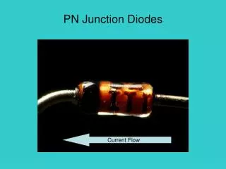
Semiconductor Devices Lecture 5, pn-Junction Diode. Content. Contact potential Space charge region, Electric Field, depletion depth Current-Voltage characteristic Depletion layer capacitance Diffusion capacitance Transient Behavior Junction Breakdown.

E N D
Semiconductor Devices • Lecture 5, pn-Junction Diode
Content • Contact potential • Space charge region, Electric Field, depletion depth • Current-Voltage characteristic • Depletion layer capacitance • Diffusion capacitance • Transient Behavior • Junction Breakdown
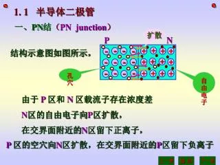
Contact potential, in Equilibrium and without applied voltage
Contact potential, in Equilibrium and without applied voltage Current density is =0 Einstein- relation
Contact potential, in Equilibrium and without applied voltage
Contact potential, in Equilibrium and without applied voltage
Contact potential, in Equilibrium and without applied voltage
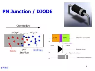
Space charge region, Electric Field Poisson’s ekvation Only fixed charge is used!
Space charge region, Electric Field The area under E(x) xn0Nd=xp0Na, W=xn0+xp0 Contact potential expressed in doping level and depletion depth
Space charge region, depletion depth What happened with xp0 and xn0 if Na or Nd is large?
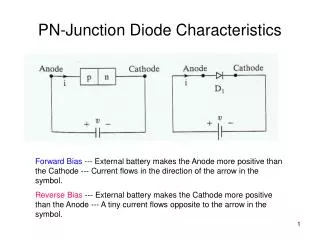
Current-Voltage Characteristic Forward biased junction: Diffusion current increase. The drift currents are almost constant
Current-Voltage Characteristic Reverse biased junction: Diffusion current decrease. The drift currents are almost constant
Current-Voltage Characteristic Generation of charge carrier in the depletion region as well as charges diffuse into the junction, swept through the depletion layer by the electric field, result into a leakage current of the device
Current-Voltage Characteristic, injection of minority carrier (forward bias) • Contact potential caused by a different concentration across the junction • With bias applied 1/2 gives
Current-Voltage Characteristic, injection of minority carrier (forward bias) Subtracting equilibrium hole and electron conc. Diffusion length
Current-Voltage Characteristic, injection of minority carrier (forward bias) Hole diffusion current at point xn Hole current injected into the n-material Electron current injected into the p-material
Current-Voltage Characteristic, the diode equation. Total current at xn=xp=0 Voltage depended minority injection included
Current-Voltage Characteristic, the diode equation. Reversed bias! Increasing Vr gives: Shockley Equation Good agreement for Ge. Bad for Si
Current-Voltage Characteristic, the diode equation. The current is constant through the component The doping affect the injection The p-doping is higher than the n-doping which gives a bigger hole injection
Current-Voltage Characteristic, 2 order effect • Generation and recombination in the depletion volume • Ohmic losses
Current-Voltage Characteristic, 2 order effect Recombination center in the bandgap. In reverse bias mode the center act as a generations center, which affect the leakage current. (b) Thermal generation of carrier in neutral region (a)
Current-Voltage Characteristic, 2 order effect • The diode equation is modified to take care of the effect of recombination. An ideality factor n with a value from 1 to 2, is therefore introduced. 1 is pure diffusion and 2 is pure recombination. A real diode is somewhere in-between. • I0’ is modified to better explain the current when recombination/generation center affect the leakage current. Generation life-time in depletion region Minority carrier lifetime in neutral n-doped region (p+n-diode)
Ohmic losses V Va
Depletion layer capacitance Def. of Capacitance 0 V bias
Depletion layer capacitance Equal amount of charge on each side, opposite charge Propagation of depletion region caused by the doping Differentiation gives the junction capacitance. The capacitance is voltage dependent and decrease with increased reverse bias Can be written as a simple plate capacitor
Depletion layer capacitance s Si: Ks=12
Diffusion capacitance Long diodes, The diode is longer than the diffusion length for the minority carrier, no contribution to the capacitance Short diodes, the most silicon diodes behave as short diodes Storage length
Transient Behavior Injection of minority carrier, when the diode is forward biased. p+n-diode
Transient Behavior After injection of carrier, the diode is reversed biased. The diode conduct until all injected carrier have recombined.
Junction Breakdown • Zener breakdown • Avalanche breakdown
Junction Breakdown, zener n and p are doped high, which result in tunneling through the potential barrier Negative temp. coeff Vb T
Junction Breakdown, Avalanche An electron is accelerated in a high electric Field , which gives impact ionization. Positive temp coeff.
Junction Breakdown, avalanche in surface High Electric Field SiO2 + + + + + + + + + + + + p - - - - - - - - - - - - Low doped n n+