Download
1 / 37
660 likes | 1.3k Vues
PN Junction. Section 2.2-2.3. Tentative Schedule. Important Dates. 2/4: Test #1 2/6: Class Canceled!. c02f01. Review. Intrinsic Semiconductor Extrinsic Semiconductor Currents Drift Current Diffusion Current. Not A Whole Lot of Free Electrons at Room Temperature. c02f03. At T=0K.

E N D
PN Junction Section 2.2-2.3
Important Dates • 2/4: Test #1 • 2/6: Class Canceled!
Review • Intrinsic Semiconductor • Extrinsic Semiconductor • Currents • Drift Current • Diffusion Current
Not A Whole Lot of Free Electrons at Room Temperature c02f03 At T=0K Electrons gain thermal energy and break away from the bonds. They begin to act as “free charge carriers”—free electron.
c02f05 Add Phosphorous to Silicon to Create an silicon Phosphorus has 5 valence electrons. The 5th electron is “unattached”. This electron is free to move and serves as a charge carrier.
Add Boron to Silicon to Create a p-type Silicon c02f06 if we dope silicon with an atom that provides an insufficient number of electrons, then we may obtain many incomplete covalent bonds. A boron has only 3 valence electrons and can form only 3 covalent bonds. Therefore, it contains a hole and is ready to absorb a free electron.
Two Ways to Produce Currents Mechanism: Electric Field Mechanism: Concentration Gradient
Drift Current Drift current is composed of the drift current due to holes and the drift current due to electrons. Drift current is caused by the presence of an electric field.
c02f11 if charge carriers are “dropped” (injected) into a semiconductor so as to create a nonuniform density. Even in the absence of an electric field, the carriers move toward regions of low concentration, thereby carrying an electric current so long as the nonuniformity is sustained.
Diffusion current due to Holes Where does the – sign come from?
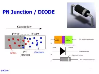
c02f16 Cathode Anode (p-type) (n-type) What do we get by introducing n-type and p-type dopants into two adjacent sections of a piece of silicon?
c02f31 IS=Reverse Saturation=leakage current
Creation of Depletion Region c02f19 Each e- that departs from the n side leaves behind a positive ion. Electrons enter the P side and create neg. ion. P side is suddenly joined with the n side The immediate vincinity of the junction is depleted of free carriers.
c02f20 PN Junction Without Bias Voltage Electric field within the depletion region points from the left to the right. The direction of the electric field make it difficult for more free electrons to move from the n side to the p side. Equilibrium does not mean that there is no movement of carriers, but instead We have the gradient to push holes to the left. E is there to push the drift current to the right.
Electric Field/Voltage Definition of Voltage: The work done in moving a unit positive charge in an electric field. Alternative definition: - + Vo Caution: You can’t use Vo as a battery!!!
c02f21 (P is neutral, even though it carries 5 electrons, one of them being a free electron.) (B is neutral, even though it carries 3 electrons. ) Net charge =0 Net charge =0 E depends on the net charge included in the imaginary surface. Extra Credit: Derive Built in Voltage
Different ways of Crossing PN Junction Diffusion Diffusion np=ni2 Drift Drift Majority carriers cross the pn junction via diffusion (because you have the gradient) Minority carriers cross the pn junction via drift( because you have the E, not the gradient)
PN Junction under Reverse Bias Reverse: Connect the + terminal to the n side. Depletion region widens. Therefore, stronger E. Minority carrier to cross the PN junction easily through drift. Current is composed mostly of drift current contributed by minority carriers. np to the left and pn to the right. Current from n side to p side, the current is negative. E
PN Junction as a capacitor Smaller capacitance. (More charge separation) Large capacitance. (Less charge separation) As the reverse bias increases, the width of the depletion region increases.
c02f25 Bias dependent capacitance. Useful in cell phone applications. c02f25
Forward Bias Diode Depletion region shrinks due to charges from the battery. The electric field is weaker. Majority carrier can cross via diffusion; Greater diffusion current. Current flows from P side to N side
c02f28 Equilibrium Forward Biased Diode Majority carriers cross the junction via diffusion. Minority carriers increased on both sides of the junction.
c02f29 (gradient of minority carriers) nn,f enters the p side as minority carriers (np,f). np,f will recombine with the pp,f, which are abundant.
c02f30 ID must be constant at all points along x In the vincinity of depletion region, the current consists mostly of minority carriers because you have the gradient! Away from the depletion region, the current consists mostly Of majority carriers. At each point along the x-axis, the two components add up To Itot. (This is the bottom line)
c02f31 IS=Reverse Saturation=leakage current
Measure Forward Biased Diode Current Listed R1=330 Ohms, Measured R1=327.8 Ohms, % error=-0.66 %
Reverse Biased Diode IS=Reverse Saturation=leakage current
Dynamic Resistance Dynamic Resistance from the measurement: (0.748-0.70)/(13.8 mA-5.74 mA)= 48 mV/8.06 mA =5.95 Ohms From the manufacture’s specification=8.33 Ohms, using data from 0.7V and 0.725 V in Figure 4.
c02f33 If VD is less than VD, On, the diode behaves like an open circuit. The diode will behave like an open circuit for VD=VD,on
Reverse Bias Measured R2 is 0.997 MOhms. % Error is about -0.3 %