Download
1 / 14
140 likes | 312 Vues
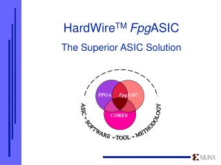
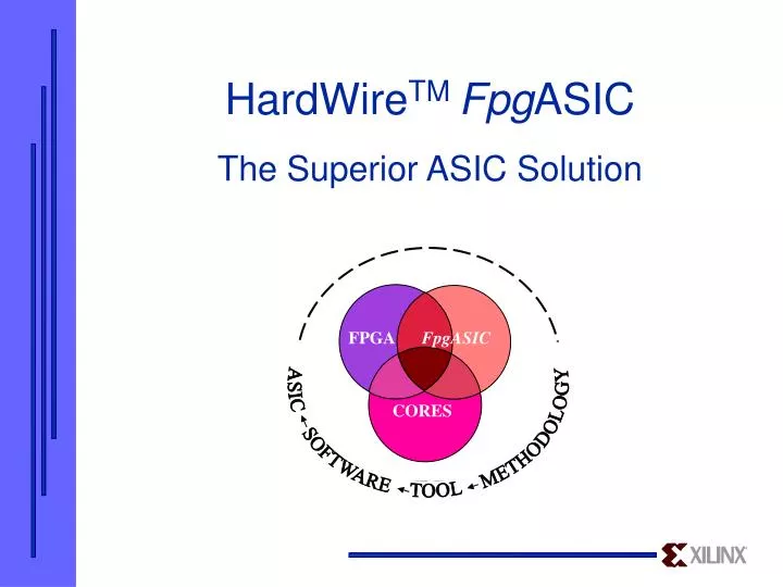
FPGA. FpgASIC. CORES. HardWire TM Fpg ASIC The Superior ASIC Solution. Agenda. Conversion Experience Success Stories Conversion Process Conversion Time. Xilinx Has Seven Years of FPGA Conversion Experience. Over 800 Xilinx FPGA’s Converted Over 5 Million Devices Shipped

E N D
FPGA FpgASIC CORES HardWireTM FpgASICThe Superior ASIC Solution
Agenda Conversion Experience Success Stories Conversion Process Conversion Time
Xilinx Has Seven Years of FPGA Conversion Experience • Over 800 Xilinx FPGA’s Converted • Over 5 Million Devices Shipped • >95% first-time-right Prototypes • Experience with Complex Designs • PCI • High RAM Usage • Asynchronous Clocks
HardWire Success Application: Arcade Video Game FPGA: XC4020E-2PQ208 Features: Dual port RAM, PCI Logicore (Initiator and Target) Comment: Attempted to do standard ASIC with several manufacturers with no success. Solution: Only the HardWire ASIC solution was able to incorporate the logic and features providing a cost effective solution. HardWire Device: XC4420-PQ208C Projected Volume: 120-200KU per year.
HardWire Success Application: Controller chip in three chip telecom chipset. FPGA: XC4020E-3PQ208I Features: Dual port RAM, JTAG and Configuration Emulation. Comment: Needed fast time to market cost effective solution. Internal solution could not meet time to market requirements. Solution: HardWire ASIC provided production quality samples 7 weeks after the design submittal kit was received. Including package change. HardWire Device: XC4420-TQ100C Projected Volume: 100-300KU per year. Sold to several phone companies
HardWire Success Application: six chip encryption chipset for next generation phone/radio base station. FPGA: XC3030-5PC84I, XC5204-4PQ100, XC4005E-3PQ100. Features: SelectRAM, JTAG and Configuration Emulation. Comment: Limited engineering resources available to complete conversion process. Time to completion critical for end customer. Solution: Used different HardWire technologies to match features and performance with most cost effective solution. Production quality samples delivered 6 weeks after complete design submittal kit received. HardWire Device: XC3330-PC84I, XC5404-PQ100I, XC4405-PQ100C Projected Volume: 10-20KU per year.
Ensure Conversion Success • Use good ASIC design practices • Fully synchronous design methodology • Acceptable timing margins in chip periphery • Position GND pins to avoid problems with simultaneous switching outputs • Fully test designs in the FPGA • Run Design Rule Check - make sure there are no errors • Communicate Requirements as Soon as Possible • RAM/JTAG/Configuration Emulation • I/O drives and slew rate • Any special timing issues • Submit Clear, Accurate, Complete Documentation
HardWire Conversion Flow Customer XILINX • Design Submittal: • Form • Design file • Schematic • Design Check • DesignLockTM Conversion • Timing Analysis • TBLK Insertion Design Sign-off • Build Prototype: • Vector Generation • Mask Generation • Fab, Assembly, Test Evaluate & Approve Proto HardWire Production
HardWire DESIGNLOCK Conversion Reduces Re-design Risk FPGA HardWire All CLBs and nets are preserved - No netlist transformation Unused CLB/logic is not mapped for optimal die size CLBs & nets are maintained in the same relative location on the die.
HardWire CLB Based Mapping Preserves Functionality CLB Mapping Preserves Placement ASIC Place and Route is Random By Design
DesignLocktm Methodology Minimizes Change HardWire ASIC DesignLocktm Methodology: Placement, Routing and Relative Timing Preserved FPGA DEVICE ROUTING Generic ASIC Routing Can Change Critical Paths
Complete Submittals Speed Conversion • Completed Design Submittal Form • Disk containing all files: .LCA, .MBO,.BIT, .XRP files for XACT (.NCD, .BIT, .BITSTREAM files for M1) • A board- level schematic showing FPGA pinouts • NRE purchase order
HardWire Conversion Time is a Function of FPGA Density 1997 1998 Average design density 5 – 20KG 50 – 100KG Total conversion time 2-4 weeks 5 – 10 weeks Average gates per week 2-5KG 10 – 15KG
Conversion Time Set Expectations Early * Add queue time, add customer sign-off/evaluation time.