Download
1 / 25
250 likes | 440 Vues
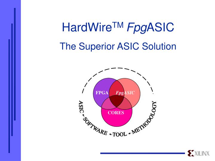
FPGA. FpgASIC. CORES. HardWire TM Fpg ASIC The Superior ASIC Solution. Agenda. Mission HardWire Features Roadmap Selector Guide Architecture Issues & Solutions for ASIC Users Availability. Mission. Help our customers with faster time to market and

E N D
FPGA FpgASIC CORES HardWireTM FpgASICThe Superior ASIC Solution
Agenda Mission HardWire Features Roadmap Selector Guide Architecture Issues & Solutions for ASIC Users Availability
Mission Help our customers with faster time to market and flexible product life cycle management through programmable logic solutions of software, application engineering and silicon Software Silicon Application Engineering
ASIC Alternatives Custom Highest Density ASIC Tools ASIC Xilinx Product Line Custom Transparent Conversion 100% Tested FpgASIC Programmable GA Architecture High Density ASIC Tools FPGA Programmable PAL Architecture Medium Density PAL-like Tools CPLD Programmable AND/OR Architecture Low Density Simple Tools PAL™
FPGA Design Advantages ASIC Test VectorGeneration40% • Reduced Simulation Requirements • Hardware Verification • Concurrent Development of System Hardware and Software • Highly Flexible • No Test Vector Generation • No Prototype or Re-spin Leadtime Test VectorGeneration 40% Simulation 25% Schematic Capture10% Prototype Test10% Vendor Interface10% Specifications - 5% ASIC Design Time by Task * Source: Integrated Circuit Engineering Corporation, 1996
FpgASIC Conversion The Xilinx Advantage “Design-Once” HardWire ASIC FPGADesign FpgASIC • Fast Development • Time-to-Market • Concurrent Engineering • Flexibility • No Customer Re-design • No Customer Vectors • All FPGA Features • Mask Programmed Pricing • Fastest Time from Design Concept to Low-cost Silicon
Xilinx FPGA + FpgASIC Advantage“Design Once” Powerful Unique Xilinx Logic Methodology Logic Design FPGA Implementation FPGA ASIC Implementation “Make” Non-Turn-key “Buy” Turn-Key FpgaASIC Implementation Option FpgASIC ASIC Xilinx Holds the Patent on “FPGA Conversion Without Re-Design”
Xilinx Introduces the FpgASICXH3 HardWire ASIC Family • Built in Xilinx Features • Package Optimized Die Sizes • Same Proven DESIGNLOCK Flow • Performance Optimized for Xilinx FPGA’s • Competitive With Commercial ASIC’s
XH3 ArchitectureThe Cutting Edge of Technology • XH3/XH3L uses high-performance ASIC core • Technology from Silicon Architects (SiArc) division of Synopsys • Similar technology used by 20+ semiconductor companies • XH3 Architecture (built-in FPGA features) unique to Xilinx • 6 patents filed
HardWire ASIC Technology Roadmap • XH4 • 0.25/ 0.18Technology • FPGA-specific Architecture • High Performance/Embedded Cores • Advanced Mapping • XH3 • 0.5/ 0.35 Technology • First FpgASIC • High performance/Size-optimized • ASIC Core • “DesignLock 3” • HW2 • 0.6Technology • Sea of Gates Architecture (S.O.G.) • Die Size Optimized • “DesignLockTM” Conversion Methodology • HW1 • 0.8 Technology • FPGA Replica • Single Mask Personalization • “Direct-Map” Conversion 1999 1997 1998 1994 1992
DEVICEXH302 XH304 XH306 XH308 XH310 XH312 DLM USABLE 14,000 25,000 45,000 70,000 90,000 140,000 GATES MAX PADS136 172 204 240 292 352 PACKAGES PC84 TQ144 PQ160 PQ240 PQ240 SUPPORTED PC84 PQ100 PQ208 BG225 BG225 PQ304 PQ100 TQ100 BG256 BG256 BG352 TQ100 VQ100 HQ304 BG432 VQ100 TQ144 BG352 PQ160 E/EX XC4005 XC4010 XC4013 XC4020 XC4025 XC4028 FPGAs XC4008 XC4013 XC4020 XC4025 XC4028 XC4036 SUPPORTED XC4010 XC4025 XC4028 XC4036 XC4013 XH3 Family Product Support
XH3 Architecture is Xilinx Specific FPGA Features POR, CE VREF, CLKS FPGA I/O (Driver, ESD, 5V Tolerant, JTAG) Core FPGA Cores Efficient Hi-Performance ASIC Core PAD Core OSC
HardWire CLB Based Mapping Preserves Functionality CLB Mapping Preserves Placement ASIC Place and Route is Random By Design
DesignLocktm Methodology Minimizes Change HardWire ASIC DesignLocktm Methodology: Placement, Routing and Relative Timing Preserved FPGA DEVICE ROUTING Generic ASIC Routing Can Change Critical Paths
DesignLockTM Emulates Xilinx FPGA I/O • Read Xilinx FPGA bitstream • Apply verified FpgASIC IOB model for each IOB in FPGA design • Result: FpgASIC IOBs function like FPGA IOBs • Risk reduced. Predictability increased • JTAG same as FPGA - no change to manufacturing test program IOB IOB IOB IOB IOB IOB Logic IOB IOB IOB IOB IOB IOB IOB IOB
DesignLockTM Provides Universal Configuration Emulation • ASIC vendors don’t understand FPGA operation • ASIC vendors try to emulate FPGA functionality (if possible) • ASIC flow is time consuming and error-prone • Xilinx holds patent on Configuration Emulation PROG PROG FPGA FpgASIC DONE DONE M0 M0 Configuration Emulation Logic Configuration Logic M1 M1 M2 M2 Address / Data Address / Data
FpgASIC RAM models Xilinx FPGA RAM ASIC vendors rely on their own models => Risk factor Only Xilinx FpgASIC hasRAM Init RAM Block Testability RAM Initialization DPRAM Asynchronous RAM Synchronous HardWire Conversion Provides All SelectRAM Options 100% test coverage
FPGA FPGA + HardWire ASIC FPGA + Generic ASIC Generic ASIC The Competitive Battleground Reducing Time to Volume Design/ Verification System Verification Iterations ASIC Re-engrg. Prototypes Iterations Production Iterations Iterations (ASIC) With Iterations With Iterations Iterations (ASIC)
Typical Product Life Cycle Model • Design and prototype with FPGA • Production ramp in FPGA during FpgASIC conversion • FPGA for production upsides & system E-O-L UNPLANNED UPSIDE PROGRAMMABLE VOLUME PRODUCTION RAMP-UP VOLUME END-OF-LIFE HardWiire FpgASIC
Typical Product Life CycleFPGA + HardWire ASIC Reduces the Risk • Re-design flexibility with FPGA • Initial production with FPGA • Convert to HardWire when code is stable UNPLANNED UPSIDE PRODUCTION RAMP WITH FPGA END-OF-LIFE HARDWIRE FpgASIC ENHANCEMENTS WITH OFF-THE SHELF FPGA PROTOTYPE & SYSTEM VERIFICATION PRODUCT FAILS
FPGA + HardWire + ASIC Advantage 20X 10X 5X 2X 1X Xilinx FPGA Xilinx HardWire FpgASIC Generic ASIC Generic ASIC Re-engineering Cost (Risk, Resources, Time to Market) High Zero
HardWire Methodology Reduces Risk Typical ASIC Design Phases Xilinx HardWire Methodology T e s t D e v e l o p m e n t Complete FPGA Design I t e r a t i o n s Re-Capture Complete FPGA Design Verification Place and Route Xilinx ATPG Simulation Physical Data Base Design Conversion Physical Data Base Production Ready Prototypes Prototypes
Key Differentiator Customer Benefit DesignLock™ No verification/simulation Same I/O as FPGA Same start-up timing Same RAM as FPGA No test vectors to write FpgASIC Architecture FPGA Compatibility Turn-key Conversion No customer resources FpgASIC Differentiation vs. ASIC
HardWire FpgASIC Availability * 1st Production submittals