Download
1 / 20
220 likes | 257 Vues
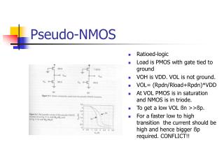
NMOS Amplifiers. 1. Music for your ears. Musique 101. Audio Spectrum. Amplifiers have limited bandwidth frequency response of Amplifiers.

E N D
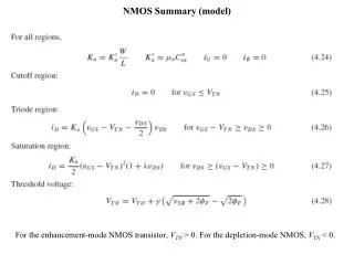
Amplifiers have limited bandwidth frequency response of Amplifiers Constant gain between w1 & w2 (Bandwidth) ; otherwise lower gain. Amp chosen so its BW coincides with required spectrum to be amplified … otherwise signals distorted Figure 1.21 Typical magnitude response of an amplifier. |T(v)| is the magnitude of the amplifier transfer function—that is, the ratio of the output Vo(v) to the input Vi(v).
Voltage Amplifier - Transfer characteristic Can also have circuit Amps output input Figure 1.11 (a) A voltage amplifier fed with a signal vI(t) and connected to a load resistance RL. (b) Transfer characteristic of a linear voltage amplifier with voltage gain Av.
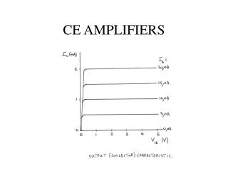
MOSFET AMP common source Graphical method Using load line :: slope is 1/RD For any value of VI = VGS Locate corresponding ID – VDS curve Find vo Figure 4.26(a) Basic structure of the common-source amplifier. (b) Graphical construction to determine the transfer characteristic of the amplifier in (a).
MOSFET Amp. Biased at Q • Xfer characteristic • inverting • Similar to switch characteristic • Biased at point Q • Vi superimposed on VIQ • Vi small linear amp operation VO proportional to Vi Figure 4.26(Continued)(c) Transfer characteristic showing operation as an amplifier biased at point Q.
MOSFET as linear Amp – use saturation seg. • How to select Bias point • Q1 bias point • Not enough +ve swing • Too close to Vdd • Q2 bias point • Too close to triode • Insufficient –ve swing Figure 4.27 Two load lines and corresponding bias points. Bias point Q1 does not leave sufficient room for positive signal swing at the drain (too close to VDD). Bias point Q2 is too close to the boundary of the triode region and might not allow for sufficient negative signal swing.
Some Amplifiers Require 2 supplies Eg 2 supply +ve & -ve swings Figure 1.12 An amplifier that requires two dc supplies (shown as batteries) for operation.
output Amplifier transfer characteristics Amps have limitations .. may saturate ..signal (2) L+ >= A*vi Amp linearity desired Vout(t) = A * Vin(t) input Figure 1.13 An amplifier transfer characteristic that is linear except for output saturation. Two power supplies used
Amplifier Biasing – ensures linearity Nonlinear response Figure 1.14 (a) An amplifier transfer characteristic that shows considerable nonlinearity. (b) To obtain linear operation the amplifier is biased as shown, and the signal amplitude is kept small. Observe that this amplifier is operated from a single power supply, VDD. 12
Inverting Amplifier biasing example Top limit = 10v, lower limit = 0.3v Output 180 degrees out of phase with input L+ =~ 10v @ Vt = 0 For 5 V bias @ Vo = 5v Vt = 0.673 L- = 0.3v Vt = 0.690 Figure 1.15 A sketch of the transfer characteristic of the amplifier of Example 1.2. Note that this amplifier is inverting (i.e., with a gain that is negative).
Voltage Amplifier Circuit Model used for simulation, circuit analysis Inp. resistance Out. resistance Inp. source, / Rs Load RL Gain = Aw; input resistance = Ri, Output resistance = Ro vo = Aw * vi * RL/(RL + Ro) ; effect of output resistance Ro vo / vi = Aw * RL/(RL + Ro) ; voltage gain vi = vs * Ri / (Ri+ Rs) ; effect of Ri vo / vs = Aw * Ri / (Ri + Rs) * RL/(RL + Ro); overall voltage gain accounting for input / output impedances Figure 1.17 (a) Circuit model for the voltage amplifier. (b) The voltage amplifier with input signal source and load.
More Gain ? Use Cascaded stages Ex 1.3 Input stage needs high input impedance Output stage needs low output impedance Input resistance of a stage = load resistance of previous stage Vi1 / Vs = 1 M / ( 1M + 100k) = 0.909 ; effect of 1st Rin Av1 = Vi2 / Vi1 = 10 * 100k / (100k + 1k) = 9.9 ; gain 1st stage, A = 10 Av2 = Vi3 / Vi2 = 100 * 10k / (10k + 1k) = 90.9 ; gain 2nd stage, A = 100 Av3 = VL / Vi3 = 1 * 100 / ( 100 + 10) = 0.909 ; gain 3rd stage, A = 1 Av = VL / Vi1 = 9.9 * 90.9 * 0.909 = 818 ; 3 stage gain VL / Vs = 818 * 0.909 = 743.6 ; from source to load Ideal Gain = 10 * 100 = 1000 Figure 1.18 Three-stage amplifier for Example 1.3.
Amplifiers have limited bandwidth frequency response of Amplifiers Constant gain between w1 & w2 (Bandwidth) ; otherwise lower gain. Amp chosen so its BW coincides with required spectrum to be amplified … otherwise signals distorted Figure 1.21 Typical magnitude response of an amplifier. |T(v)| is the magnitude of the amplifier transfer function—that is, the ratio of the output Vo(v) to the input Vi(v).
Capacitively Coupled Amplifier Stages Figure 1.27 Use of a capacitor to couple amplifier stages.
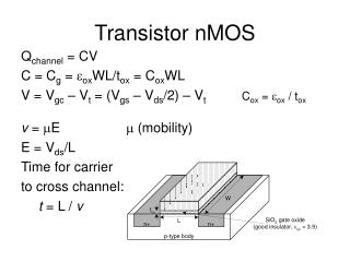
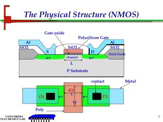
An NMOS Common Source Amplifier Amp. Circuit Xfer Characteristic Figure 4.26(a) Basic structure of the common-source amplifier. (b) Graphical construction to determine the transfer characteristic of the amplifier in (a). 18
NMOS common source Amp. Cont’d Xfer Characteristic Biased at point Q Figure 4.26(Continued)(c) Transfer characteristic showing operation as an amplifier biased at point Q. 19
Pspice Amplifier Example Figure 4.63 Capture schematic of the CS amplifier in Example 4.14.