Download
1 / 17
680 likes | 3.58k Vues
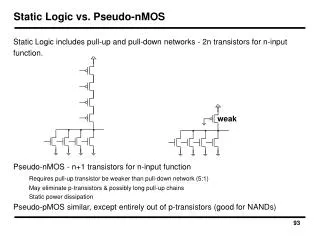
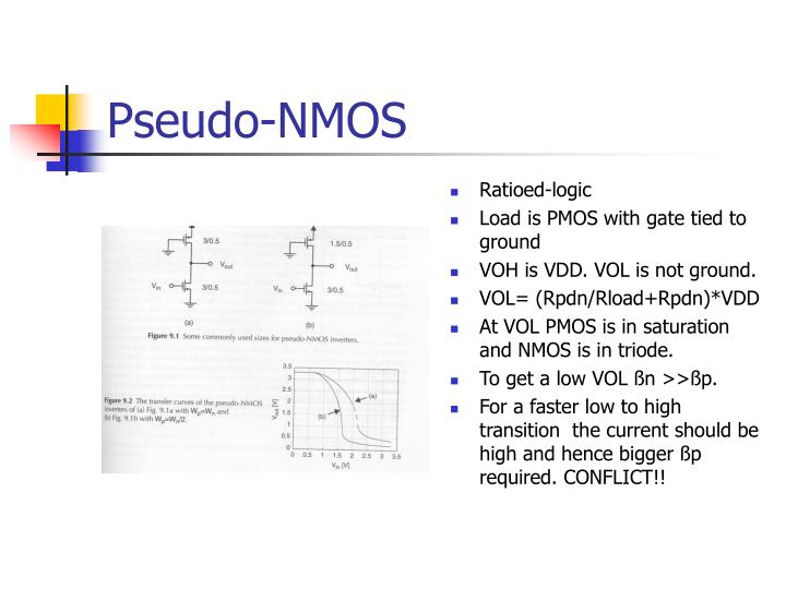
Pseudo-NMOS. Ratioed-logic Load is PMOS with gate tied to ground VOH is VDD. VOL is not ground. VOL= (Rpdn/Rload+Rpdn)*VDD At VOL PMOS is in saturation and NMOS is in triode. To get a low VOL ßn >>ßp.

E N D
Pseudo-NMOS • Ratioed-logic • Load is PMOS with gate tied to ground • VOH is VDD. VOL is not ground. • VOL= (Rpdn/Rload+Rpdn)*VDD • At VOL PMOS is in saturation and NMOS is in triode. • To get a low VOL ßn >>ßp. • For a faster low to high transition the current should be high and hence bigger ßp required. CONFLICT!!
Problems and Advantages of Pseudo-NMOS Problems : Voltage transfer characteristic is asymmetrical Rise and fall time are asymmetrical Static power consumption Advantages: High speed Useful when designing complex gates with large fan-in.
Dynamic Combinational Logic • Avoids static power dissipation • Uses a sequence of pre-charge and Evaluate to realize complex logic functions. • The inputs to the logic are not allowed to change and are zero in pre-charge phase. • Pre-charge phase when phi=0 and Evaluate when phi=1. • If the output is discharged it can not be charged again. • tpLH=0! And tpHL depends on the pull down network.
Advantages of Dynamic Combinational logic over static combinational logic • Number of transistors are less N+2 compared to 2N. • Non-Ratioed. • No static power consumption • High switching speed.
Problems Associated with dynamic logic • Charge leakage • Charge sharing • Clock feed through
Cascading Dynamic gates • Problem arises when Dynamic gates are cascaded. • The PDN of second stage is in a conducting stage. This leads to faulty operation of the gates. • Correct operation is guaranteed as long as the inputs make a single 0-1 transition.
Domino Logic • Consists of a Phin block followed by a static inverter. • Inverter ensures that there is only 0-1 transition during evaluation mode. • During pre-charge all inputs a(except external inputs) ate set to zero. During Evaluation the output of first domino stays at 0 or makes a 0-1 translation affecting the second domino. • Only non-Inverting logic can be implemented. • Very high speeds can be achieved. • Useful for large fan-out circuits like ALU.
NP-CMOS • Faster than domino logic because of the elimination of static inverters • The inverter can be avoided by exploiting the duality between the phin and phip blocks. • Phip and phin blocks are clocked with inverse clock to make evaluation and pre-charge time coincide.
Dynamic Sequential Logic C2MOS Latch • Insensitive to clock overlap. • Made of Phi and Phib sections • When phi=1 , phi is in evaluation mode and phib in hold mode. • When phi=0, phi is on hold and phib in evaluation.
Dynamic sequential Circuits NORA – CMOS • For implementing Fast Pipelined data-path • Combines C2MOS registers and np-CMOS dynamic logic. • Logic and Latch clocked in such a way that both are simultaneously in evaluation or hold( precharge ) mode
Dynamic sequential Circuits • C2MOS based circuit is race free as long as all the logic functions implemented between latches are non-inverting. • During overlap only pull-up or pull-down is activated. • Figure shows a 1-1 overlap.The only way race can happen is if the function is inverting.
Dynamic sequential Circuits • Figure shows phi and phib modules. • When phi=0 for phi block logic is in precharge and latch is in Hold and for phib block logic and latch are in evaluate. • When phi=1 for phi block logic and latch are in evaluate and for phib block logic is in precharge and latch in hold. • Consists of chain of alternating phi and phib blocks.
Dynamic sequential logic Design rules for NORA-CMOS • Inputs to the dynamic phin( phip) block are allowed to make only a single 0-1(1-0) transition. • In order to avoid races the number of inversion between latches should be even. • If dynamic nodes nodes are present , the number of static inverters between latch and dynamic gate in logic block should be even.
True Single Phase Clocking • Only a single clock is needed to correctly operate a dynamic-sequential circuit. • The latches are modified as shown • For a doubled n-C2MOS latch when phi is high, the latch is in evaluation and when phi is low it is in hold. • All constraints are removed. • Races are eliminated.
TSPC • As shown in the figure the logic can be implemented inside the latch or between the latch. • The latch can be further modified so that the clock load is reduced by half and the number of transistors reduced. • Not all nodes experience full voltage swing in this case.
TSPC • D-Flip Flop implementation using TSPC.