Download
1 / 74
870 likes | 1.61k Vues
Properties of Digital Circuits. Quantized States Voltage Transfer Characteristic (VTC) Voltage Levels Noise Margins Current Levels Fan-In and Fan-out Power Dissipation Propagation Delay Power-Delay Product IC Packaging Technology Trends of MOS Microprocessors and Memories.

E N D
Properties of Digital Circuits • Quantized States • Voltage Transfer Characteristic (VTC) • Voltage Levels • Noise Margins • Current Levels • Fan-In and Fan-out • Power Dissipation • Propagation Delay • Power-Delay Product • IC Packaging • Technology Trends of MOS Microprocessors and Memories ECE 3450 M. A. Jupina, VU, 2009
Some Key Lecture Objectives • Before performing the Properties of Digital Circuits practicum, we need to look at the key properties of digital circuits used to compare one technology with another. • How voltage levels of a technology not only define the logic states of a technology, but also lead to a definition of noise immunity for a technology. • An understanding of how current levels, “loading,” power dissipation, and speed of operation are all inter-related. Reference: Fundamentals of Digital Logic, Chap 1, Sec 3.8, and App E.4. ECE 3450 M. A. Jupina, VU, 2009
Transistor-Transistor-Logic (TTL) TTL dominated the IC market from the 1960’s to early 1980’s. This picture changed in the 1980s due to two major factors: • Discrete logic gates in static CMOS became competitive in speed at a lower power cost. • The advent of programmable logic components such as PLDs and FPGAs made it possible to program complex random logic functions (equivalent to hundreds of TTL gates) on a single component. This results in a large reduction in board real-estate cost, while adding flexibility. ECE 3450 M. A. Jupina, VU, 2009
CMOS • CMOS stands for Complementary Metal-Oxide Semiconductor. MOS field-effect transistors (n-channel and p-channel) are used to construct logic gates. • FETs are voltage controlled and operate nearly as an ideal switch. • MOSFETs advantages: Lower power consumption than BJTs so billons of devices can be packed onto a single chip (MOSFETs dimensions are in the sub-micron range). ECE 3450 M. A. Jupina, VU, 2009
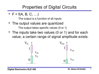
Quantized States • Binary System possible states: 1 or 0, on or off positive logic: 1= high, 0 = low negative logic: 1= low, 0 = high • Future Systems – multilevel logic Ex: if three different on-off levels, then 23 = 8 logic states ECE 3450 M. A. Jupina, VU, 2009
VTC of an Inverter Vi Vo Voltage Levels (VOH, VOL, VIL,VIH) are defined at dVo/dVi = -1 ECE 3450 M. A. Jupina, VU, 2009
VTC for a CMOS Inverter V out V = V Slope = – 1 OH DD V = 0 V OL ( ) V V V V – V V T IL IH DD T DD V in V DD — 2 ECE 3450 M. A. Jupina, VU, 2009
Table of Voltage Levels for TTL Families ECE 3450 M. A. Jupina, VU, 2009
PSPICE Schematic of LS7404 TTL Inverter ECE 3450 M. A. Jupina, VU, 2009
PSPICE VTC Simulation of the LS7404 ECE 3450 M. A. Jupina, VU, 2009
PSPICE VTC Simulation of the LS7404 VIL = 0.7 V VIH = 1.18 V VOH = 4 V VOL = 0.15 V ECE 3450 M. A. Jupina, VU, 2009
Digital Properties PracticumMeasured VTC of LS7404 ECE 3450 M. A. Jupina, VU, 2009
Voltage Level Definitions • VIH – High Level Input Voltage Vinput≥VIH to be recognized as a “1” • TTL Ex: VIH = 2V, thus at the input a “1” is between 2V and VCC ECE 3450 M. A. Jupina, VU, 2009
Voltage Level Definitions • VOH – High Level Output Voltage • TTL Ex: VOH = 2.4V, thus at the output a “1” is between 2.4V and VCC ECE 3450 M. A. Jupina, VU, 2009
Voltage Level Definitions • VIL – Low Level Input Voltage Vinput≤ VIL to be recognized as a “0” • TTL Ex: VIL = 0.8V, thus at the input a “0” is between 0V and 0.8V ECE 3450 M. A. Jupina, VU, 2009
Voltage Level Definitions • VOL – Low Level Output Voltage • TTL Ex: VOL = 0.4V, thus at the output a “0” is between 0V and 0.4V ECE 3450 M. A. Jupina, VU, 2009
Logic Level Matching Levels at output of one gate must be sufficient to drive next gate. VOH > VIH VOL < VIL ECE 3450 M. A. Jupina, VU, 2009
Voltage Level Definitions • VLS – logic swing at the output VLS = VOH - VOL • Ideally, should be as large as possible. Higher VLS reduces ambiguity in the output logic state and increases noise immunity. • VLS defines the range of output voltages that define the unknown state, “X” state. ECE 3450 M. A. Jupina, VU, 2009
Voltage Level Definitions • VTW – transition width at the input VTW = VIH - VIL • Ideally, should be as small as possible. Lower VTW reduces ambiguity in the input logic state and increases noise immunity. • VTW defines the range of input voltages that define the unknown state, “X” state. ECE 3450 M. A. Jupina, VU, 2009
Voltage Levels Summary “1” “X” “0” “1” “X” “0” ECE 3450 M. A. Jupina, VU, 2009
v(t) i(t) VDD Noise in Digital Circuits • Noise – unwanted variations of voltages and currents at the logic nodes • from two wires placed side by side • capacitive coupling • voltage change on one wire can influence signal on the neighboring wire • cross talk • inductive coupling • current change on one wire can influence signal on the neighboring wire • from noise on the power and ground supply rails • can influence signal levels in the gate ECE 3450 M. A. Jupina, VU, 2009
Noise Margin Definitions • NM’s define the amount of noise immunity in the high or low level logic state. • NMH - High Level Noise Margin NMH = VOH - VIH • NML - Low Level Noise Margin NML = VIL - VOL • Ideally, the NM’s should be as large and as equal as possible. • NM of a technology = min{NMH , NML} • TTL Ex: NMH = 2.4V - 2V = 0.4V NML = 0.8V – 0.4V = 0.4V ECE 3450 M. A. Jupina, VU, 2009
Noise Superimposed on TTL Signals OR ECE 3450 M. A. Jupina, VU, 2009
Noise Margin Question A certain logic family has the following voltage parameters: VIH = 1.18 V, VOH = 4 V, VIL = 0.7 V, VOL = 0.15 V What is the largest positive-going noise spike that can be tolerated? What is the largest negative-going noise spike that can be tolerated? NML = VIL – VOL = 0.55V NMH = VOH – VIH = 2.82V ECE 3450 M. A. Jupina, VU, 2009
PSPICE Noise Simulation Demonstrating the Concept of Noise Margin (LS7404) ECE 3450 M. A. Jupina, VU, 2009
PSPICE Noise SimulationV(IN) = Source + Noise VOH VOL Vpeak-to-peak ECE 3450 M. A. Jupina, VU, 2009
PSPICE Noise SimulationV(OUT) for Vpeak= 0, 0.5, 1, 3.1V Vpeak=0V Vpeak=0.5V Vpeak=1V Vpeak=3.1V ECE 3450 M. A. Jupina, VU, 2009
The Ideal Inverter The ideal gate should have • infinite slope (gain) in the transition region • high and low noise margins equal to half the logic swing • a gate threshold located in the middle of the logic swing • input and output impedances of infinity and zero, respectively • infinite output drive capability (infinite output current or fanout) VOUT Ideal VTC VCC = VSUPPLY VTW=0 (Impossible to be in X state) VOH = VCC NMH = NML = Ri = Ro = 0 Fanout = VCC/2 VLS=VCC VOL = 0V VIN VIL=VIH= VCC/2 ECE 3450 M. A. Jupina, VU, 2009
Current Level Conventions Current out of a terminal is given as a negative value in Data Sheets. Current into a terminal is given as positive value in Data Sheets. ECE 3450 M. A. Jupina, VU, 2009
Table of Current Levels for TTL Families ECE 3450 M. A. Jupina, VU, 2009
Current Sourcing Versus Current Sinking ECE 3450 M. A. Jupina, VU, 2009
Current Level Definitions “0” • IOL – Low Level Output Current Maximum current that an output terminal of a gate can sink when the output is “0”. If |IOUT| > |IOL|, then eventually VOUT > VOL • TTL Ex: IOL = +16mA, VOUT≤ 0.4V IOUT ECE 3450 M. A. Jupina, VU, 2009
Current Level Definitions “0” • IIL – Low Level Input Current Maximum current that an input terminal of a gate can source when the input is “0”. • TTL Ex: IIL = -1.6mA, VIN≤ 0.8V IIN ECE 3450 M. A. Jupina, VU, 2009
Current Level Definitions “1” • IOH – High Level Output Current Maximum current that an output terminal of a gate can source when the output is “1”. If |IOUT| > |IOH|, then eventually VOUT < VOH • TTL Ex: IOH = -400mA, VOUT ≥ 2.4V IOUT ECE 3450 M. A. Jupina, VU, 2009
Current Level Definitions “1” • IIH – High Level Input Current Maximum current that an input terminal of a gate can sink when the input is “1”. • TTL Ex: IIH = +40mA, VIN≥ 2.0V IIN ECE 3450 M. A. Jupina, VU, 2009
TTL Example – LED Load Which circuit would you use to drive an LED? (Assume that VLED = ~1.7 V.) I + - 1.7 V I - + 1.7 V ECE 3450 M. A. Jupina, VU, 2009
TTL Example – LED Load Analysis of the first circuit: I + - 1.7 V For this circuit, Vout≥2.4V and thus I ≥ 2mA > IOH ! (IOH = -0.4mA) This TTL logic device can’t supply this amount of current since the output voltage will decrease as the output current exceeds IOH. Thereby, a “1” state at the output is no longer guaranteed. ECE 3450 M. A. Jupina, VU, 2009
TTL Example – LED Load Analysis of the second circuit: I - + 1.7 V If Vout = 0.4V, then I = 9 mA < IOL. ( IOL = 16 mA ) If Vout = 0V, then I = 10 mA < IOL. The necessary output current can be supplied. For TTL, the magnitude of IOL > the magnitude of IOH ECE 3450 M. A. Jupina, VU, 2009
Fan-out – number of load gates connected to the output of the driving gate • gates with large fan-out are slower N • Fan-in – the number of inputs to the gate • gates with large fan-in are bigger and slower M Fan-Out and Fan-In ECE 3450 M. A. Jupina, VU, 2009
Static or DC Fan-Out • Fan-Out (N) is defined as the number of loads (gate inputs) that can be driven by a single gate output at DC or low frequencies. • Low Level Fan-out NL = • High Level Fan-out NH = • N = min{NL,NH} • Ex: For most TTL families, N = NL. ECE 3450 M. A. Jupina, VU, 2009
TTL Static Fan-Out Example ECE 3450 M. A. Jupina, VU, 2009
Dynamic Fan-Out Additional current due to the capacitive load. The impedance of a capacitor, (wC)-1, decreases as the frequency increases. Therefore, the load current increases as the frequency increases. This additional load current must be taken into account when determining fan-out at high frequency. Dynamic Fan-Out << Static Fan-Out ECE 3450 M. A. Jupina, VU, 2009
Power Dissipation Definitions Instantaneous power: p(t) = v(t)i(t) = Vsupplyi(t) Peak power: Ppeak = Vsupplyipeak Average power: ECE 3450 M. A. Jupina, VU, 2009
Power Dissipation • Power consumption: how much energy is consumed per operation and how much heat the circuit dissipates • power supply sizing (determined by peak power) Ppeak = Vsupplyipeak • battery lifetime (determined by average power dissipation) p(t) = v(t)i(t) = Vsupplyi(t) Pavg= 1/T p(t) dt = Vsupply/T isupply(t) dt • packaging and cooling requirements • Two important components: static (DC) and dynamic CMOS Example: PAV = VDD Ileakage + CL VDD2 f ECE 3450 M. A. Jupina, VU, 2009
TTL Supply Currents • The power supply current is dependent on the output state. • ICCL > ICCH since • IOL > IOH • IIL > IIH Note: these values are for a 7400 NAND Gate chip (total current for 4 NAND gates) ECE 3450 M. A. Jupina, VU, 2009
Power Dissipation of a TTL Gate ECE 3450 M. A. Jupina, VU, 2009
Power Dissipation of a TTL GateExample What is the power dissipation of a single TTL NAND gate (7400)? ECE 3450 M. A. Jupina, VU, 2009
Power Supply Currents Versus Frequency 10 KHz 100 KHz 1 MHz 10 MHz 100 MHz ECE 3450 M. A. Jupina, VU, 2009
Propagation Delay Time Vin Vout A measure of how long it takes for a gate to change state. Ideally, should be as short as possible. tPHL - the time it takes the output to go from a high to a low tPLH - the time it takes the output to go from a low to a high Average Propagation Delay Time tp = ECE 3450 M. A. Jupina, VU, 2009
Modeling Propagation Delay R Model circuit as a first-order RC network vout C vin V 0 Vout (t) = (1 – e–t/)V ,where = RC Time to reach 50% point is t = ln(2) = 0.69 t ECE 3450 M. A. Jupina, VU, 2009