Download
1 / 24
250 likes | 418 Vues
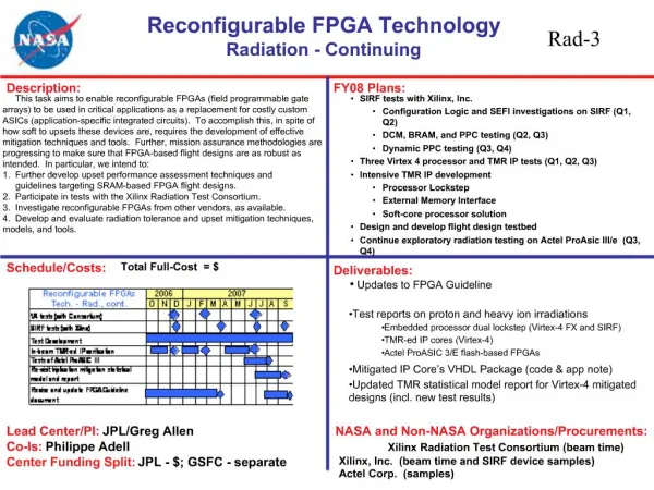
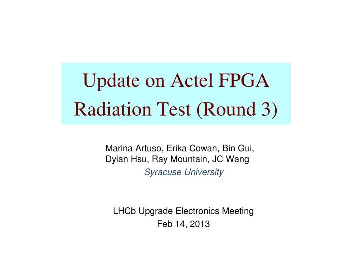
Update on Actel FPGA Radiation Test (Round 3). Marina Artuso , Erika Cowan, Bin Gui , Dylan Hsu, Ray Mountain, JC Wang Syracuse University LHCb Upgrade Electronics Meeting Feb 14, 2013. Introduction. Radiation test facility @ NPTC, Mass . General Hospital .

E N D
Update on Actel FPGA Radiation Test (Round 3) Marina Artuso, Erika Cowan, Bin Gui, Dylan Hsu, Ray Mountain, JC Wang Syracuse University LHCb Upgrade Electronics Meeting Feb 14, 2013
Introduction • Radiation test facility @ NPTC, Mass. General Hospital. • Proton primary beam 230 MeV, maximum intensity 2.1x10¹¹ p/cm2/s. • Beam energy range 70-230 MeV using single or double Pb foil scattering, essentially monochromatic. • Beam spot diameter varies from 1 cm, 2.5 cm, to10 cm. • Dosimetry: ~5% precision by beam ionization chamber calibrated by Faraday cup. • Test beam line: collimating aperture, intensity control. • Align the device under test with beam line using laser alignment reference. • We had 3 rounds of beam tests using this facility. The earlier two are mainly SEU tests. In the latest one we have both PLL & SEU tests. • PLL test with 4 FPGA chips (Actel 3APE1500‐2 ). • SEU test with 2 FPGA chips (Actel3APE1500). • This presentation focuses on the PLL test only. We want to see if FPGAs function up to ~30 kRad. The study is in progress. Plots & numbers are preliminary. preliminary
Irradiation Facility: NPTC @ MGH FAR STATION 10 m CYCLOTRON quads bend NEAR STATION ~ 220 MeV Protons FPGA BEAMLINE 3
Cyclotron (Louvain #00) quads Experiment room dipoles
Gentry Room Main Control Room Neurosurgical Room Control Room 3 Full beam control this round
Near station 2 x PC run labview DAQ 2 x TNG 5 provide communication between PC & FPGA, and current measurements. Far station Laptop PCs to control near station DAQ PCs via a local network.
Our local contact Ethan Cascio
Aperture Ø12.7 mm FPGA Board Ion Chamber p Beam Adjustable mechanics
Front Back Alignment Laser spot
Beam On FPGA • With one Pb foil scattering. Beam energy 226 MeV. • Particle flux uniformity is better than 10% in a 10 mm diameter. The size is ideal for our FPGA tests ( dice size: 7.9 x 7.7 mm2 ). • Beam is centered on FPGAs, aligned with laser spot. • We test 2 FPGAs are a time. The downstream (back) FPGA receives ~ 68% radiation dose comparing to the upstream (front) one. ~28 mm (pkg) Relative Flux Position (cm) Proton Radio-Chromatograph
PLL Test Setup Check if frequencies of produced clocks are correct By Albert Zwart Twisted pair cable provides delay for TDC to measure Measure 40 MHz time signal, with 1280 MHz equivalent precision. Version # ? Generate two 320 MHz and one 80 MHz clocks of fixed phases, Set a 5-bit number for comparator to check against measured TDC. Check if measured TDC value agrees with U13/14.
TDC Logic & Time Diagram 320 MHz Relative phases provided by WilcoVink hit arrival signal of the next operation falling edges of clk_80 (clk40=1) shreg0,1 pipelined into reg0,1 falling edges of clk_40 shreg2,3 pipelined into reg2,3 rising edges of clk_0 L-shfit shreg0, shreg0[7]=hit combine 4 independent operations Setups at NIKHEF & Syracuse both work with this version of firmware.
Result From NIKHEF Test Setup 40 MHz (25 ns) as base clock 39.84 MHz (25.1 ns) as hit. In this way, the delay time is gradually shifted. TDC bits TDC value changes gradually from 0 to 31 Non-uniform width (in time) is due to the not-perfect phase difference between the two 320 MHz clocks, and their duties. Snapshots by Tom Sluijk & WilcoVink TDC value
TDC vs Delay Before Radiation From LED Step width ~ 0.78 ns • TDC value vs delay follows an expected step structure. • We made a bunch of twisted cables with length varying between 15 to 150 cm. • Delay cables are connected in normal or reversed polarities. The net effect is 12.5ns extra (less) delay if the signal is perfectly 50% duty. • We use cable delay plus an offset as the total delay. The offset reflects contributions from gates & traces. It is obtained to align the points to the steps, andis slightly chip dependent. • Points at step edges may be at transition of two TDC values and is difficult to determine from LED. This is better studied with large statistics of TDC-error counts. • Cable delay will be better calibrated. Cables during beam test: 36.1& 36.6 cm TDC=10. Cable Delay + offset
What Has Been Recorded? • PLL / TDC test is done in small runs. • In each run 233 TDC measurements are compared with preset comparator value (U13/U14). We count the number of times that the two are different. Triple voting is applied to counter to minimize the beam effect on counting. • During a run it is also recorded whether or not there is a PLL clock error or a PLL lock error at any time. • The 34 bit TDC-error counter, 1 bit PLL_clock_error , 1 bit PLL_lock_error & 2 dummy bits are packed to a 38-bit data. • At the end of each run the 38-bit data is buffered and the next run starts immediately after that. Meanwhile FPGA sends serial data to PC. • A run lasts for 215 s (233/40 MHz). • During beam test we have one run with beam and the next without. In this way the beam data is more reliable. • The current consumed by each FPGA test board is recorded continuously. The data is under analysis. • After a few beam runs, we run firmware verification & reconfiguration.
Integrated Radiation Dose Chips are tested in pairs FPGA 4 (front) & FPGA 3 (back). FPGA 2 (front) & FPGA 1 (back). FPGA J (front) & FPGA L (back). The radiation dose a downstream (back) FPGA receives is ~68% that of its upstream partner. All FPGAs receives 30 kRad or more, except for FPGA 1 that we intentionally removed for other test.
FPGA 1: TDC Errors Counts & Other Checks Verification OK Verification failed Reconfiguration failed x3 Verification failed Power cycle Reconnect programmer Verification failed Change programmer Power cycle Verification failed x2 Reconfiguration failed Programmer was disconnected from boards during beam time. Blue lines separate runs. The TDC errors for each run can be at any time. Verification OK Reconfiguration OK Verification OK After 17.9 kRad, FPGA 1 is taken out. We want to keep it alive to compare transition curves before & after irradiation. 22 6 1
FPGA 2: TDC Errors Counts & Other Checks Verification failed Reconfiguration failed x3 Power cycle Reconfiguration failed PLL lock error. The run was with high intensity Verification OK Reconfiguration OK Verification OK Change comparator value to 11; Large error count is seen. Change back to 10. Near station Computer crashed LED indicates TDC = 12 FPGA 2 received 45.6 kRad 1.2x10⁹ 38 1 37
FPGA 3: TDC Errors Counts & Other Checks Verification failed x3 Reconfiguration failed x3 Power cycle Reconnect programmer Verification failed Reconfiguration failed Verification: OK Reconfiguration: OK LEDs look fine Verification OK Reconfiguration OK FPGA 3 received 30.9 kRad. 4.8 x 10⁴ 59 1 6
FPGA 4: TDC Errors Counts & Other Checks FPGA 4 was not stable even before the test beam. Its firmware is slightly different from others. Otherwise TDC is non-linear. Verification & reconfiguration failed before the beamtest started. Only 36 (out of 38) bits readout. LED indicates TDC=11 Power cycled TDC remained 11 Set comparator to 11 Communication totally failed LED indicates TDC=0 clock_error is on FPGA 4 received 47.8 kRad 4.6 x 10⁷ 8.5 x 10⁶ 7.9 x 10⁵ 5.3 x 10⁵ 1.6 x 10⁴ 504 511 ~64 1 23
Post Irradiation FPGA Tests • The FPGA chips are tested after irradiation. • Firmware verification and reconfiguration. • At the end of beam test all 4 chips failed.They still can not be verified or reconfigured. • Example of error messages: code 0x8052 failed to enter programming mode;code 0x805A verify failed at row 5643, code0x8056, fail to program UROW. • Even though the firmware can not be verified or reconfigured, 3 out of 4 chips seem still functioning as TDC. • Chip1: no particular problem at the end of test beam. With same setting now it has prob(TDC 11)=6.8x10⁻⁹, prob(TDC 9)=0, prob(TDC 10) ~ 1. • Chip2: at the end of test beam, LED indicated TDC = 12 instead of 10. The problem is gone now. Prob(TDC 11)=1.1x10⁻⁶, prob(TDC 9)=0, prob(TDC 10)~1. • Chip3, no particular problem at the end of test beam other than TDC-errors. Now prob(TDC 11) = 0.023, prob(TDC 9) = 0, prob(TDC 10)=1-0.023. • Chip4, LED indicated TDC=0 & PLL_clock_error at the end of testbeam. Now PLL_clock_ error disappeared. When comparator is set to TDC=0, LED indicates not TDC-error, consistent with readout. When set TDC 0, TDC-error LED is on but readout number is funny suggesting that the counter may fail. • Special chip 4
FPGA 1 Probability Curve Comparison Before Irradiation After Irradiation • We measure TDC value probability vs delay curves. • After irradiation the transition areas are wider than before. The center might also shifted. • The cable delays are calculated from their physical lengths of twisted pairs, which are expected to be not precise. • We tried to calibrate the cable delay with electronics signals to the precision of a few 10 ps. The outcome is not great.
Calibration of Cable Delay R. Kiesleret al, NIM 56 (1967) 357. Discriminator Measure period Cable under study The measurement is stable to the precision < 10ps. However, the difference with length measurement may be too big. We may have a way to refine these measurement. Suggestions are welcomed.
Summary • We performed radiation test on Actel FPGA chips. • With four 3APE1500‐2 chips we test PLL / TDC performance and measured TDC error rate. • All four chips can not be verified or reconfigured after certain radiation dose. The TDC error rate increases. One chip stops functioning as TDC. • We start post-irradiation tests.The cable calibration method needs to be refined. TDC vs delay curve calibration is done on FPGA 1, and needs to be done on FPGA 2 & 3. • Current measurement and SEU data need to be analyzed (combined with the first 2 rounds). • Annealing process will be applied. • A write-up will be started soon.