Download
1 / 9
90 likes | 198 Vues
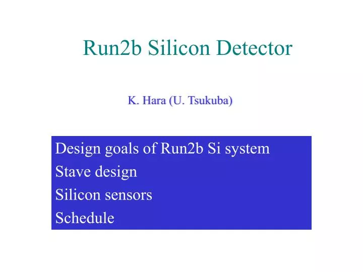
Run2b Silicon Detector. K. Hara (U. Tsukuba). K. Hara (U. Tsukuba). Design goals of Run2b Si system Stave design Silicon sensors Schedule. Design goals of Run2b silicon. Performance as good as/better than Run2a system Simple and robust* , to be ready by summer 2004

E N D
Run2b Silicon Detector K. Hara (U. Tsukuba) K. Hara (U. Tsukuba) Design goals of Run2b Si system Stave design Silicon sensors Schedule
Design goals of Run2b silicon • Performance as good as/better than Run2a system • Simple and robust*, to be ready by summer 2004 • No changes for DAQ chains new (Si, chip-hybrid, mini-portcard, Junction PC) SVX3 chips: Honeywell! (cost, yield), noise@large Cdet SVX4 chips: 0.25μm process, 2.5V, submitted before Christmas Fine-pitch hybrid (BeO) developed for L00 Eliminate rad-critical (~5.7fb-1)DOIMs in Run2a portcard *Uniform stave design(~90%)+special inner layer+a la L00 Minimum use of light-weight cables
6-fold layout 106.5R(SVX2a) 163.5R L1 axial coverage~0.7? 6-fold wedge SVT 90°@L1,2,5 good anchor to COT good ΔZ for 3D impact param
Descoping? Use outer staves for L1 Drop L4 or L5 4%change ~3 GeV less MH reach ~14% more L
RunIIBStave water channel Peek tube hybrid substrate C fiber cable bus readout chip pitch adapter Silicon detector • Stave structure (60 cm long, supported at z=0 and ±60cm): • Carbon fiber – rohacell structure with ~2x6 mm peek cooling pipes • On each side: • 6 single sided silicon sensors • 3 hybrids glued to the silicon. • Silicon glued to copper-kapton bus cables • Hybrids wirebonded to bus cables Mini Portcard
Number of Sensors Outer axial (75um) 1008 °(93um) 504 2.5°(80um) 504 3 types 2016 Inner axial 144 axial’ 72 ° 72 3 types 288 ? 90 90 Micron (13+α)months @+200/mo HPK:2300+spares=2700
Si sensor : R&D issue • Axial and SAS sensors are similar to ATLAS • 90°on 6” process is new via SiO2 insulator Previously achieved: ~4μm (4” SSDM) ~5μm (4” DSDM) ? (6” SSDM)
Schedule 2002 2003 2004 Shutdown (6months) mechanical prototypes(Mar~May) electrical prototypes(~Sept) full production(200d) stave production Si prototypes 90deg R&D barrel assembly final tests order production Si series Si delivery SVX4, cables, others Schedule risks: (1) SVX4 chip (for electrical prototyping, reliability) successful operation w/ bus cable (2) installation in 6-mon shutdown Contingency ~6 months