Download
1 / 18
180 likes | 279 Vues
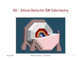
Silicon Detector EM Calorimetry. SD (Silicon Detector). Conceived as a high performance detector for NLC Reasonably uncompromised performance But Constrained & Rational cost

E N D
Silicon DetectorEM Calorimetry LC Workshop M. Breidenbach
SD (Silicon Detector) • Conceived as a high performance detector for NLC • Reasonably uncompromised performance • But • Constrained & Rational cost • We accept the notion that excellent energy flow calorimetry is required, and explore optimization of a Tungsten-Silicon EMCal… LC Workshop M. Breidenbach
Silicon Tungsten EMCal • Figure of merit something like BR2/s, where s is the rms sum of Moliere radius of the calorimeter and the pixel size. • Maintain the great Moliere radius of tungsten (9 mm) by minimizing the gaps between ~2.5 mm tungsten plates. Dilution is (1+Rgap/Rw) • Could a layer of silicon/support/readout etc fit in a 2.5 mm gap? Even less?? 1.5 mm goal?? • Requires clever electronic-mechanical integration! LC Workshop M. Breidenbach
EMCal, continued • Diode pixels between 5 – 10 mm square on largest hexagon fitting in largest available wafer. (6” available now – 300 mm when??) Consider m tracking as well as E flow in picking pixel dimension. • Develop readout electronics of preamplification through digitization, zero suppression and IO on bump bonded chip. Upgrade would be full integration of readout on detector wafer. (R&D opportunity!) • Optimize shaping time for small diode capacitance. Probably too long for significant bunch localization within train. But some detector element needs good time resolution!!! LC Workshop M. Breidenbach
Channel Counts [Forget Them!!] • We are used to pixel counts in CCD’s … • 3x10⁸ last time, 1x10⁹ this time, no problem • Silicon Strip Tracker ~5x10⁶ strips (channels??) • EMCal ~5x107 pixels (channels??) • Don’t even think about multiplying channels by O($10)…… • Must solve the cluster technology challenges. LC Workshop M. Breidenbach
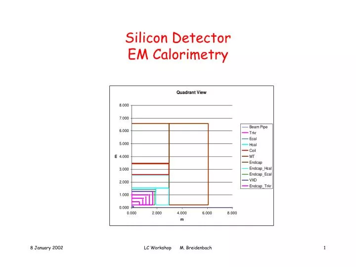
Structure LC Workshop M. Breidenbach
Gross System Architecture Silicon Diode Array Readout Chip Network Interconnect LC Workshop M. Breidenbach
Pixels on 6” Wafer LC Workshop M. Breidenbach
Zoom to Readout Chip LC Workshop M. Breidenbach
Cross Section LC Workshop M. Breidenbach
Signal Collection from m2 board LC Workshop M. Breidenbach
G1 M U X 12 bit ADC Shaper G2 G3 Preamplifier Architecture • Charge amplifier and shaper followed by three amplifiers with gains G1,G2,G3 and sample & holds. • Comparator logic to select appropriate range • Mux and 12 bit ADC LC Workshop M. Breidenbach
Noise and Muons • Assume 300 m (400-500 m possible) effective e- collection at 80 e-/m. s=0.6%. So S/N=5 seems rational goal. • 1 SD noise would be 4800 e-. Assuming diode capacitance of 1 pf/mm2, and amplifier noise of 20e-/pf+200 – get about factor of two safety! (1 MIP = 2 x 10⁴ e-) LC Workshop M. Breidenbach
Plausible Resolution Criteria • Spread the 0.6% muon s into several bins, with enough range for MIP counting to a few. • Preliminary Monte Carlo indicates peak ionizing track density from a high energy shower to be 2200 µ equivalent. (5 x 10⁷ e- = 8 pC.) • Do not degrade resolution of calorimeter! Energy resolution of a sampling calorimeter with 2/3 X0 plates will not exceed 12%/√E. Say this peak should be spread over 5 bins, and take no credit for multiple sampling. LC Workshop M. Breidenbach
Low end resolution requirements • Res 1 Bin Width=50e-, Emax=1.9 Gev, Mips=8.5 LC Workshop M. Breidenbach
Required Resolution • Res 2 Bin Width=1300 e-, Emax=50 GeV,Mips=225 • Res 3 Bin Width=13000 e-,Emax=512 GeV,Mips=2325 LC Workshop M. Breidenbach
Technical Issues • Assuming integrator full scale voltage of around 1 V, feedback (and calibration) capacitors need to be ~10 pF. This is large for an integrated capacitor, but doable with substantial real estate. • Plus is that this makes the bump bond pitch easy! • Cooling: GLAST system is ~2 mW/channel. Assume 1000 pixels/wafer and power pulsing duty factor for NLC of 10-3 (10 µsec @120 Hz). HD18 (95%W, 3.5% Ni, 1.5% Cu) is possible alloy. σ=18gm/cm3, σc=0.33 w/cm-0C. Assume cooling on one edge, then ΔT=~2.50C. This is fine, but it sure doesn’t work without power pulsing!!! Need to consider possibility of copper layer in the G10. LC Workshop M. Breidenbach
Plans • We (Oregon and SLAC) plan to develop this design in more detail and (hopefully) build prototype wafers and chips. • If successful, develop board level chip. • Build 1 wafer wide by about 25 X0 deep calorimeter for test beam. LC Workshop M. Breidenbach