Download
1 / 26
330 likes | 568 Vues
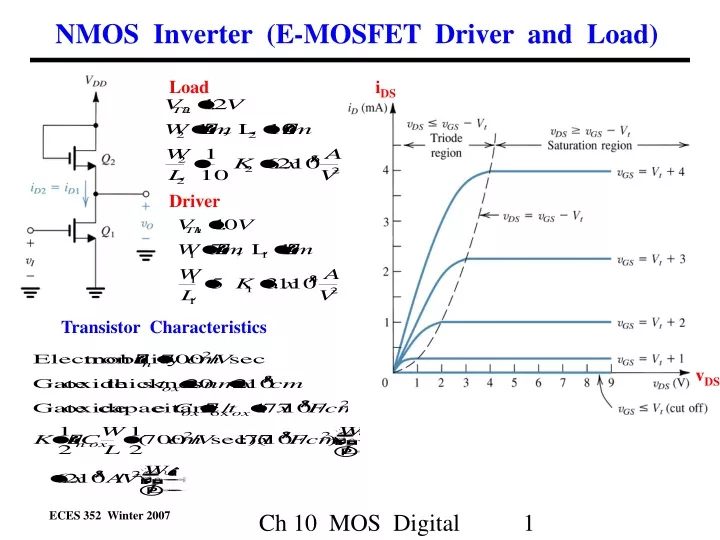
NMOS Inverter (E-MOSFET Driver and Load). Load. i DS. Driver. Transistor Characteristics. v DS. NMOS Inverter (E-MOSFET Load Transistor). Load transistor has its gate connected to its drain so v DS2 = v GS2 (Always)

E N D
Ch 10 MOS Digital – Pt. 2 NMOS Inverter (E-MOSFET Driver and Load) Load iDS Driver TransistorCharacteristics vDS
NMOS Inverter (E-MOSFET Load Transistor) • Load transistor has its gate connected to its drain so vDS2 = vGS2 (Always) • Triode-saturation boundary at vDSsat2 = vGS2 - VTh2 • Since VTh2 > 0, for load transistor vDS2 > vDSsat2 = vGS2 - VTh2 =vDS2 - VTh2 • So load transistor is ALWAYS in saturation ! It cannot operate in the triode region ! • Load’s drain current is always given by • So load transistor looks like a variable resistance of size G D S iDS2 0.08 0.06 0.04 0.02 vDS2 Ch 10 MOS Digital – Pt. 2
Ch 10 MOS Digital – Pt. 2 NMOS Inverter (E-MOSFET Driver and Load) • Voltage transfer characteristic (Vo vs Vi) • Region I (A to B) • 0 < Vi< VTh1 • iD1 = 0 since drive transistor Q1 is off, i.e. in cutoff. • iD2 = 0 since iD2 = iD1 and iD1= 0 • Output voltage is given by Vo= VDD-VDS2 = VDD-VGS2 = VDD-VTh2 = 5V- 1.2V = 3.8V • Why not 5V ? Assuming a capacitance load on the output, when Q1 (driver) turns off, then Q2 (load) provides current to charge up the capacitance C so the output Vo can rise towards VDD. • As Vo rises, VDS2 (still = VGS2) decreases. • When VGS2 decreases to VTh2, then Q2 turns off and stops supplying the charging current, so Vo cannot rise further. • So Vo cannot rise above VDD - VTh2 = 3.8V Load Driver C vo 5V I A B 3.8V 0 vi VTh1 =1.0V 0 5V
Ch 10 MOS Digital – Pt. 2 NMOS Inverter (E-MOSFET Driver and Load) • Region II (B to C) • Driver comes on in saturation mode • Load always in saturation mode. Load Driver vo iDS1 5V Driver B A 3.8V I II A to B C C 0 vi vDS1 VTh1 =1.0V 0 5V
Ch 10 MOS Digital – Pt. 2 NMOS Inverter (E-MOSFET Driver and Load) • Where is point C? • Driver transistor operating in saturation mode in region II, so point C is where it leaves saturation, i.e. where vDS1 = vo = vDSsat1 = vGS1 - VTh1 = vi - VTh1 iDS1 vo A B 3.8V I II A to B C C 0.47V 0 vDS1 vi 1.47V 0 VTh1 =1.0V 5V
NMOS Inverter (E-MOSFET Driver and Load) • Where is the equivalent resistance that the load transistor provides in region II ? • Recall the load transistor acts like a load resistor with an effective resistance • At point B, vo = 3.8 V and the load transistor is off so • At point C, vo = 0.47 V so iDS1 vo A B 3.8V I II A to B C C 0.47V 0 vDS1 vi 1.47V 0 VTh1 =1.0V 5V Ch 10 MOS Digital – Pt. 2
Ch 10 MOS Digital – Pt. 2 NMOS Inverter (E-MOSFET Driver and Load) • Region III (C to D) • Driver in triode mode Load Driver vo iDS1 5V A B 3.8V D I II III A to B C C D 0.47V vi 0 vDS1 1.47V 0 5V VTh1 =1.0V
Ch 10 MOS Digital – Pt. 2 NMOS Inverter (E-MOSFET Driver and Load) • Region III (C to D) Point D vo iDS1 5V A B 3.8 V D I II III 0.47 V A to B C C D 0.05 V 0 vi vDS1 1.47 V 3.8 V 5V 0 VTh1 =1.0 V
Ch 10 MOS Digital – Pt. 2 Noise Margins for NMOS Inverter (E-MOSFET Driver and Load) • Noise margin for low state • Measures degree of inverter sensitivity to noise for the low state, i.e. how large a noise signal causes problems. • Assumes identical inverter providing input signal • Noise Margin = NML = VIL - VOLwhere • VOL= output voltage when input set to VOH • VIL= maximum input voltage recognized as a low input • For this inverter design, NML is much larger than for resistor load case! • Can changeNML by changing K’s or VTh1. high high low vo 5 V NML= VIL - VOL =1.0V- 0.05V = 0.95V VOH = 3.8 V VOL= 0.05V vi 5 V VIL=VTh1 = 1.0V Vi =VOH = 3.8 V Vi =VOL = 0.05V
Ch 10 MOS Digital – Pt. 2 Noise Margins for NMOS Inverter (E-MOSFET Driver and Load) • Noise margin for high state • Noise Margin = NMH = VOH – VIHwhere • VOH= output high voltage when input set to VOL • VIH = minimum input voltage recognized as a high input • Maybe findVIH by using vo(vi) for region II (Q1 in saturation). Recall • So must findVIH by using vo(vi) for the device in region III. low low high vo I II III NMH= VOH - VIH = 3.8 V- 1.53 V = 2.27 V VOH = 3.8 V Slope = -1 Vo= 0.32 V vi VOL= 0.05V Vi =VOH = 3.8 V VIH=1.53 V
Ch 10 MOS Digital – Pt. 2 NMOS Inverter (E-MOSFET Driver and Load) Load • Load transistor Q2 acts as a variable load resistance. • Since VTh2 > 0 for load transistor (enhancement type), and vDS2 = vGS2 then vDS2 > vDSsat2 = vGS2 - VTh2 =vDS2 - VTh2 • So load transistor is ALWAYS in saturation mode, so its current is • Effective resistance of Load Q2 is Driver iDS1 Load line for variable load resistance. D A to B C vDS1
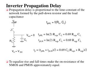
Ch 10 MOS Digital – Pt. 2 Propagation Delays and Switching Times for NMOS Inverters Load • Output goes from Low to High • Driver Q1 turns off • Load Q2 provides current to charge up C. iD2 iC Driver C iD1 * Output goes from High to Low * Driver Q1 turns on to discharge C (So vi = VOH = 3.8 V) * Driver initially in saturation mode, then triode mode * Load Q2 produces current that must be absorbed by Q1. These equations are not as easily integrated to find vo (vi ). Saturation Triode
Ch 10 MOS Digital – Pt. 2 Propagation Delay for NMOS Inverter • Output goes from High (VOH = 3.8V) to Low (VOL = 0.05V) • DriverQ1 (starts from P R S T) • At outset, Q1 is off (P), and vDS1 = vo = VOH = 3.8V, vi < VTh1 • Driver turns on (P toR) when vGS1 is switched to VOH = 3.8 V. • Driver initially in saturation mode, then moves into triode as capacitor discharges and vDS1 decreases as Q1 moves along constant vGS1 characteristic (R S T). • Q1 ends at (T) , where vGS1 = vi= 3.8V and vDS1 = vo = VOL = 0.05V. • Load Q2 (goes from R’ S’ T’) (always in saturation) Load iD2 iC Driver C iD1 Driver Load iDS1 iDS2 T’ 0.08 vGS2 = vDS2 = VDD-VOL = 4.95V 0.06 R vGS1 = 3.8 V S S’ 0.04 0.02 vGS2 = vDS2 = VDD-VOH = 1.2V T P vDS1 vDS2 R’ P’ vo =VOL = 0.05 V vo =VOH = 3.8 V
Ch 10 MOS Digital – Pt. 2 Approximate Analysis of Propagation Delays • Output goes from High (VOH = 3.8V) to Low (VOL = 0.05V) • As an approximation, we use average currents for the transistors to calculate an average discharge current for the capacitor. • We select point S to be the point where the output voltage has fallen halfway from its peak value VOH to its minimum value VOL. • We define the high to low propagation time tPHL as the time it takes for the output to go from vo = vo(R) = VOH = 3.8 V to vo=vo(S) = 1/2(VOH +VOL) = 1.93 V. Load iD2 iC Driver C iD1 Driver iDS1 R S vGS1 = 3.8 V T P vDS1 vo =VOL = 0.05 V vo =VOH = 3.8 V vo =VOH = 3.8 V
Ch 10 MOS Digital – Pt. 2 Approximate Analysis of Propagation Delays • Output goes from High (VOH = 3.8V) to Low (VOL = 0.05V) • Average current for the DRIVER transistor. • At point R, vi = vi(R) = VOH =3.8V and driver is in saturation region since the output has not fallen so vo = vo(R) = VOH • At point S, • So drain current at point S is given by • So average drain current for the driver is Load iD2 iC Driver C iD1 Driver iDS1 R S vGS1 = 3.8 V T P vDS1 vo =VOH = 3.8 V vo =VOH = 3.8 V
Ch 10 MOS Digital – Pt. 2 Approximate Analysis of Propagation Delays • Output goes from High (VOH = 3.8V) to Low (VOL = 0.05V) • Average current for the LOAD transistor. • At point R’, vGS2 = VDD -VOH= 5.0V - 3.8V=1.2V and the load is in saturation but barely on so • At point S’, • So drain current at point S’ is given by • So average drain current for the load is Load iD2 iC Driver C iD1 Load iDS2 T’ 0.08 vGS2 = vDS2 = VDD-VOL = 4.95V 0.06 vGS1 = 3.8 V 0.04 S’ 0.02 vGS2 = vDS2 = VDD-VOH = 1.2V vDS2 R’
Ch 10 MOS Digital – Pt. 2 Approximate Analysis of Propagation Delays • Output goes from High to Low. • Using the average currents for the transistors we get an average discharge current for the capacitor • Defining the high to low propagation time tPHL as the time it takes for the output to go from vo = VOH = 3.8V to vo = 1/2(VOH +VOL) = 1.93V. • For a capacitance load of 10 pF, we get • This propagation delay is small since the driver’s current is much larger than the load’s current (since K1 >> K2). • NOTE: The load in this case (high to low) is delaying (slightly) the transition by supplying current which tends to charge up the capacitance load. Load iD2 iC Driver C iD1 Driver iDS1 R S vGS1 = 3.8 V T P vDS1 vo =VOH = 3.8 V vo =VOH = 3.8 V
Ch 10 MOS Digital – Pt. 2 Propagation Delay for NMOS Inverter • Output goes from Low (VOL= 0.05V) to High (VOH = 3.8V) • DriverQ1 turns off and remains off(starts from T P) • At outset, vo = VOL = 0.05V, vDS2 =VDD -vo = 5V-0.05V = 4.95V • As the load Q2 charges up the capacitor, vo increases and vDS2 (and vGS2 ) decreases, and the load Q2 goes from T’ S’ R’ (Q2 always remains in saturation). • At S’, Load iD2 iC Driver C iD1 Driver Load iDS2 iDS1 T’ 0.08 vGS2 = vDS2 = VDD-VOL = 4.95V 0.06 R S vGS1 = 3.8 V 0.04 S’ vGS2 = vDS2 = 3.07V 0.02 vGS2 = vDS2 = VDD-VOH = 1.2V T P vDS2 vDS1 vo =VOH = 3.8 V R’
Ch 10 MOS Digital – Pt. 2 Approximate Analysis of Propagation Delays • Output goes from Low (VOL = 0.05V) to High (VOH = 3.8V). • As an approximation, we use an average current for the load transistor to calculate an average charging current for the capacitor. • We select point S’ to be the point where the output voltage has risen halfway from its low value VOL to its peak value VOH. • We define the low to high propagation time tPLH as the time it takes for the output to go from vo = vo(T’) = VOL to vo=vo(S’) = 1/2(VOH +VOL). Load iD2 iC Driver C iD1 Load iDS2 T’ 0.08 vGS2 = vDS2 = VDD-VOL = 4.95V 0.06 0.04 S’ 0.02 vGS2 = vDS2 = VDD-VOH = 1.2V vDS2 R’
Ch 10 MOS Digital – Pt. 2 Approximate Analysis of Propagation Delays • Output goes from Low (VOL = 0.05V) to High (VOH = 3.8V). • Average current for the load transistor. • At point T’, vGS2 = VDD -VOL=5.0V - 0.05V = 4.95V and the load is in saturation so • At point S’, • So drain current at point S’ is given by • So average drain current for the load is Load iD2 iC Driver C iD1 Load iDS2 T’ 0.08 vGS2 = vDS2 = VDD-VOL = 4.95V 0.06 0.04 vGS2 = vDS2 = 3.07V S’ 0.02 vGS2 = vDS2 = VDD-VOH = 1.2V vDS2 R’
Ch 10 MOS Digital – Pt. 2 Approximate Analysis of Propagation Delays • Output goes from Low to High. • Use the average current for the load transistor to calculate the charging time. • Defining the low to high propagation time tPLH as the time it takes for the output to go from vo = VOL = 0.05V to vo = 1/2(VOH +VOL) = 1.93V. • For a capacitance load of 10 pF, we get • This propagation delay is very large since the load’s current is much smaller than the driver’s current (since K2 << K1). • The load transistor in this case is causing an excessivedelay in the transition from low to high output by supplying only a very small current to charge up the capacitance load. • Also, as the output voltage rises, vgs2 decreases so the load transistor supplies less and less current to charge up the capacitor. Load iD2 iC Driver C iD1 Load iDS2 T’ 0.08 vGS2 = vDS2 = VDD-VOL = 4.95V 0.06 vGS1 = 3.8 V 0.04 S’ 0.02 vGS2 = vDS2 = VDD-VOH = 1.2V vDS2 R’
Ch 10 MOS Digital – Pt. 2 Average Propagation Delay for NMOS Inverter • Output goes from High (VOH = 3.8V) to Low (VOL = 0.05V) • Driver on, providing discharge current (iD1 = 2.3 mA) • Load on, (iD2 = 0.011 mA) delaying output fall • Propagation delay tPHL=0.8 nsec. • Output goes from Low (VOL = 0.05V) to High (VOH = 3.8V). • Driver off (iD1 = 0). • Load providing charging current (iD2 = 0.055 mA) • Propagation delay tPLH = 340 nsec. • Inverter’s average propagation delay is tp Load iD2 iC Driver C iD1 Driver Load iDS1 iDS2 T’ 0.08 vGS2 = vDS2 = VDD-VOL = 4.95V 0.06 R vGS1 = 3.8 V S S’ 0.04 vGS2 = vDS2 = 3.07V 0.02 vGS2 = vDS2 = VDD-VOH = 1.2V T P vDS1 vDS2 vo =VOH = 3.8 V R’
Ch 10 MOS Digital – Pt. 2 Static Power Dissipation for NMOS Inverter • Output High (VOH = 3.8 V) • Driver off (iD1=0), Load on, but iD2= iD1 = 0. • No power dissipation in static high output mode (PH=0). • Output Low (VOL = 0.05 V). • Driver on and operating at point T (vo = 0.05 V). • Load on and operating at point T’ where iD2(T’) = 0.087 mA. • Power dissipation PL = iD2(T’)VDD = (0.087 mA) 5 V = 0.42 mW. • Inverter’s average power dissipation is PD= 1/2(PL+PH) = 0.21 mW. • Power delay product DP DP = PD tp = 0.21 mW (170 nsec) = 3.6x10⁻¹¹ J = 36 pJ. Load iD2 iC Driver C iD1 Driver Load iDS1 iDS2 T’ 0.08 vGS2 = vDS2 = VDD-VOL = 4.95V 0.06 R vGS1 = 3.8 V S S’ 0.04 vGS2 = vDS2 = 3.07V 0.02 vGS2 = vDS2 = VDD-VOH = 1.2V T P vDS1 vDS2 vo =VOH = 3.8 V R’
Ch 10 MOS Digital – Pt. 2 Comparison of NMOS Inverters • Noise Margins • NML = 0.05 V, NMH = 3.17 V • Propagation Delay • Power Dissipation • Power-Delay Product • Noise Margins NML = 0.95 V, NMH = 2.27 V • Propagation Delay • Power Dissipation • Power-Delay Product
Ch 10 MOS Digital – Pt. 2 How to Improve the NMOS Inverter? * How to reduce the tPLH ? * Increase the load current by increasing the load’s W/L ratio. * However, that increases the fall time tPHL since the load provides current that the driver must absorb to discharge the capacitor. The net effect may be some improvement in the tPD. * However, there will be an increase in the power dissipation. * Also, the noise margin for the high state will be degraded. • Noise Margins NML = 0.95 V, NMH = 2.27 V • Propagation Delay • Power Dissipation • Power-Delay Product
A Modified NMOS Inverter * Increase the load’s W/L ratio from 1/10 to 2 (20 X increase in K2 ). * New tPLH is 17 nsec vs previous 340 nsec. * New tPHL is 9 nsec vs previous 0.8 nsec. * New tPD is 13 nsec vs previous 170 nsec. * New power dissipation is 8.4 mW vs previous 0.21 mW. * New power-delay product is 109 pJ vs previous 36 pJ. * New VIH = 3.64 V vs previous 1.53 V. * New noise margin for the high state NMH = 3.8 - 3.64 = 0.16 V vs previous 2.27 V. • Noise Margins NML = 0.95 V, NMH = 2.27 V • Propagation Delay • Power Dissipation • Power-Delay Product Ch 10 MOS Digital – Pt. 2