Download
1 / 45
480 likes | 655 Vues
Bus Operations and Interfacing. Overview. Focus on the microprocessor bus Bus operations in general Device addressing and decoding Timing diagrams and timing requirements External devices: PRU, memory, other support chips Readings: Text: Chap 5, Chap 6 (Sec 2); Chap 7, Sec 1-5

E N D
Overview • Focus on the microprocessor bus • Bus operations in general • Device addressing and decoding • Timing diagrams and timing requirements • External devices: PRU, memory, other support chips • Readings: • Text: Chap 5, Chap 6 (Sec 2); Chap 7, Sec 1-5 • HC11: Sec 2.6 • E9: Appendix A
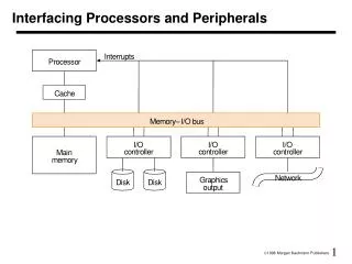
BUS Operations • This section focuses on the ability to interface external devices to the microprocessor • Interfacing requires • Hardware interface -- electrical and mechanical considerations of the interface • Software interface -- programming necessary to permit the external device and the processor exchange information • The "bus" • The set of signal lines used to connect the processor and the peripheral devices using read/write operations Cont..
BUS Operations • Can be a simple extension of the processor pins or can consist of modifications of the pins • Bus signals can be divided into 3 categories • Address • Data • Control • Figure 5.1 Processor bus organization Cont..
BUS Operations • Many microcontrollers use a multiplexed address and data bus • The data bus and (part of) the address bus use the same physical lines • Address and data signals cannot appear on the bus at the same time • Requires extra logic to demultiplex • Usually need to latch the address bits • (Temporarily put them in a register) • Why do we use a multiplexed bus? Cont..
BUS Operations • General bus operation: • Processor places desired peripheral's address onto address bus • Processor (or peripheral) places data onto data bus for a write (read) operation • Peripheral (processor) gates the data into its internal registers to complete the operation • Operation is directed by the various control lines that are included in the bus • Clock signals • Address strobe / latch • Device enable signals Cont..
BUS Operations • Data direction signals -- read vs. write • Type of reference -- standard or memory mapped I/O -- IO/M* • Data ready • The bus is not a static connection mechanism • Peripheral devices must be enabled (given access to write to the bus) only when they are participating in a data transfer • Only 1 device can be driving the bus at any given time -- otherwise bus contention results • 3-state (= tristate) devices are commonly used • Normal logic levels if enabled • High-impedance state if disabled Cont..
BUS Operations • Figure 5.3 Three-State Logic Cont..
BUS Operations • Enable signals • Usually an active-low signal • Referred to as E* • Sometimes S* or CS* • Device must be enabled before you can write to it or read from it • E* is usually derived from address lines • Other signals • R/W* • Read and Write may be separate signals • G* • Synchronizes data transfer • Sometimes CLK or E • Other address lines Cont..
BUS Operations • Address decoding • To communicate with a particular peripheral device, the processor places the device's address on the address bus • All peripherals must examine the address and decide if they are being referenced . . . • Address decoding: Usually use digital logic to generate the CS* signal • Full (exhaustive) decoding • Each peripheral is assigned to a unique address • All address bits must be used to define the referenced location • Typically used for memory devices Cont..
BUS Operations • Partial decoding • Not all address bits are used in the decoding process • Peripheral can respond to more than 1 address • Main advantage is decreased circuit complexity in the decoder • Disadvantages: • Must guard against inadvertent accesses due to multiple addresses • Somewhat inefficient use of overall address space • Example: Interface a peripheral that only uses 16 addresses • Requires 4 address bits to select 1 of the 16 internal addresses • Other system address bits used for the chip enable signal Cont.
BUS Operations • 16-bit system --12 bits for enable! • Try 6 bits for decoder instead • 74138 decoder chip is commonly used for address selection (a “1-of-8 decoder”) • 3 address bit input • 8 output select lines (active low) • 3 chip select lines (to select the 74138) Figure 5.5 74138 Decode Cheap Cont.
BUS Operations • Example: Interface two 2Kx8 memory chips to a 16-bit address system • Starting addresses for the chips should be $5000 and $6800 • Each chip has a chip enable (select) signal, E1* (active low) • Address ranges for the 2 chips are shown below • Fixed bits are routed to the decoder inputs • Varying bits are routed to the chip address lines Cont.
BUS Operations Cont.
BUS Operations • Now, use '138 output Y3 to select a 512x8 memory chip • Y3 asserted for addresses in the range $5800 to $5FFF (2KB) • 512 addresses requires 9 address bits, A0 to A8; bits A9 and A10 are not needed • As a result, partial address decoding is being used where each physical address will respond to 4 addresses • Example: address 1 in the chip is accessed whenever addresses 01011 xx 000000001 are applied to the memory system • $5801 • $5A01 • $5C01 • $5E01 Cont..
BUS Operations • Modes of operation • Internal parts of MCU: • CPU, memory, registers • External parts: • Pins for I/O and bus signals • To reduce pin count, some pins may have more than one function • For HC11, operating mode determines how pins are used • Select the operating mode using MODA and MODB pins at reset Cont..
BUS Operations • Single-chip mode • No external memory or I/O chips • Don’t need external bus • Ports B and C are used as I/O ports • Reduced system cost • Limited to on-chip RAM, ROM and EEPROM • Expanded multiplexed mode • Ports B and C used as address and data bus • Allows connections to external memory and I/O chips • Port B = A15 - A8 • Port C = AD7-AD0 (A7-A0 multiplexed with D7-D0) • Control bus signals Cont..
BUS Operations • Strobe A/address strobe pin (STRA/AS) used as AS • Strobe B/read/write pin (STRB/R/W*) used as R/W* • Special bootstrap mode • Test mode • Generally used to load in a test program, EEPROM programming, or running a monitor program • On reset, HC11 executes code located in the Boot ROM (BF00-BFFF for 68HC11E9) • Loads more program code using serial interface • Used by PCBUG11 • Listing of code in Reference Manual (Appendix B) Cont..
BUS Operations • Special test mode • Intended for use by manufacturer only • Not much documentation available • Used to test the chip • Chip specifications • Appendix A of Technical Data manual • Maximum ratings • Recommended operating conditions • DC electrical characteristics • AC electrical characteristics • Power dissipation Cont..
BUS Operations • Important when interfacing with other devices; Be aware of • Current limits • Voltage limits • Fan in/fan out • DC electrical characteristics VDD 5 V 3 V VOL Maximum low-level output voltage 0.1V 0.1V VOH Minimum high-level output voltage 4.9V 2.9V VIL Maximum low-level input voltage 1.0V 0.6V VIH Minimum high-level input voltage 3.5V 2.1V • VOL = 0.1 V Cont..
BUS operations • VOH = VDD - 0.8 V (ILOAD = -0.8 mA) • VIL = 0.2 x VDD • VIH = 0.7 x VDD • ID = 25 mA • AC electrical characteristics • Timing information
Timing diagrams and timing requirements • Timing diagrams show the changes that occur in a signal or group of signals over time • Figure 7.1 Basic timing diagram information Cont..
Timing diagrams and timing requirements • System clock • Bus transitions occur in relation to system clock • Called the E clock in 68HC11 • 1/4 crystal frequency • Low - internal process • High - reading or writing data • Some definitions: • Propagation delay: amount of time used by a device to change its output in response to an input change • Setup time: length of time that an input to a device must be stable before a clock transition • Hold time: length of time that an input to a device must remain stable after a clock transition Cont..
Timing diagrams and timing requirements • Figure 7.2 Example timing diagram for a write cycle Cont..
Timing diagrams and timing requirements tcyc 500 ns min PWEH 222 ns min tf 20 ns max tPDSU 100 ns min tr 20 ns max tPDH 50 ns min PWEL 227 ns min Cont..
Timing diagrams and timing requirements • 68HC11 timing specifications (E-series manual pages A18, 20) Cont..
Timing diagrams and timing requirements • Timing analysis and interfacing external devices to the 68HC11 • General observation: the timing characteristics of the external device (e.g., memory unit) must meet or exceed the timing requirements of the HC11 • Must compare the related timing values in the HC11 read/write timing diagram to the values in the device's diagram • Must take into account any delays due to external circuitry such as the decoder • Note that in the HC11 . . . • Address information is provided to the external device Cont..
Timing diagrams and timing requirements • (using the multiplexed address/data bus) in the low half cycle of the E-clock • Data to be read/written is placed on the data bus only in the high half cycle of the Eclock • All read and write operations MUST take place in 1 E-cycle • External devices and circuitry must be designed to meet this requirement • Cannot use “wait states” as you can in other microprocessor systems • Intel 8085: Slower devices can use READY input to request wait states • Processor maintains address, data, and control signals Cont..
Timing diagrams and timing requirements • Expanded multiplexed mode • 68HC11 supplies external bus signals • Port B = A15-A8 • Port C = A7-A0 multiplexed with D7-D0 • Address usually must be valid during entire operation • Need to latch A7-A0 (using 74HC373, for example) • Use external logic to derive control signals • Chip enable/select • Read/Write • Output enable Cont..
Timing diagrams and timing requirements • Read operation • Memory puts data on bus when clock rises • MCU latches data when clock falls Cont..
Timing diagrams and timing requirements • Write operation • MCU puts data on bus when clock rises • Memory latches data when clock falls Cont..
Timing diagrams and timing requirements • Example analysis: consider the following very general circuit layout that interfaces the HC11 to a 6264 Fast Static Ram (8k x 8) (figure shows a 6164 but we’ll use 6264 in lab) • Figure 7.6 Expanded mode operation Cont..
Timing diagrams and timing requirements • Observations on the circuit • 74373 is used as the address latch to “save” the lower 8 bits of the address that are on Port C only during the first half of the E-clock cycle • Discrete logic is used to derive the write and read enable signals for the memory chip (W* and G*) • Both can only be asserted in the second half of the E-clock cycle • 74138 is used for address decoding to generate a memory chip enable (chip select) signal (E1*) • Since the E-clock enables the 138, the decoder is only active in 2nd half cycle • Memory chip can not be enabled in the 1st half cycle • This impacts some of the timing relationships Cont..
Timing diagrams and timing requirements • Timing relationships are derived by comparing the timing diagrams of the memory chip and the HC11 and considering the external circuitry where necessary. • Read operation: • HC11: • Expects external device to place data on data bus in time for it to be read • External device must hold data until E-clock falls, but must remove it (and go to high impedance state) before HC11 places next address on bus • 6264: • Outputs data after receiving the address and the E* and G* signals Cont..
Timing diagrams and timing requirements • Timing constraints • How long does 6264 take to output data after receiving address and enable signals? • How long does it keep data on the bus? • Write operation: • 6264: • Needs address, data, E*, and W* signals • Write occurs only when both E* and W* are low • Data must be held on bus until either E* or W* rises • HC11: • Places address on address bus and latch • After E-clock rises, places data on data bus and holds it Cont..
Timing diagrams and timing requirements • Have to take into account the propagation delays due to the external circuitry • Decoder (74138): PDDEC = 25 ns • Inverter (7404): PDINV = 15 ns • Latch (74573): PDLATCH = 23 ns • Nand (7400): PDNAND = 15 ns • Read operations (read cycle 2 of 6264) Cont..
Timing diagrams and timing requirements • Timing relationships for read operation: Cont..
Timing diagrams and timing requirements • Write operations (write cycle 2 of 6264) Cont..
Timing diagrams and timing requirements • Timing relationship for write operation: Cont..
Timing diagrams and timing requirements • Timing operation for write operation(cont’d): Cont..
Timing diagrams and timing requirements • In the lab, you will be required to design and construct an expanded mode memory interface • Strongly encourage you to use Figure 2-23 in the HC11 Reference Manual as a guide • In this figure, the memory chip is always enabled • The 138 decoder is used to derive read and write enables and thus replaces the discrete logic used in Spasov’s example • Both methods will (and have) worked in the lab but using the 138 for write/read signals is recommended • Fewer chips -- all fit on a single strip of protoboard • Shorter runs of inter-chip wires • Timing analysis equations must be updated to reflect the circuit that you design! Cont..
Timing diagrams and timing requirements • Cycle-by-cycle operation • Appendix A of Reference Manual shows cycle-by-cycle execution for each instruction • Shows contents of address and data buses during each cycle • Example: STAA (ext) Cont..
Timing diagrams and timing requirements Cycle Addr Bus Data Bus R/W* 1 OP B7 1 2 OP+1 hh 1 3 OP+2 ll 1 4 hhll (A) 0 • Example: STAA (IND, X) Cycle Addr Bus Data Bus R/W* 1 OP A7 1 2 OP+1 ff 1 3 FFFF -- 1 4 X+ff (A) 0 Cont..
Timing diagrams and timing requirements • General ideas of bus expansion and interfacing • Bus composition and components • Addressing bus devices • Decoding bus addresses • Timing diagrams • HC11 interfacing and timing requirements • Modes of operation