Download
1 / 1
10 likes | 113 Vues
A=0. A=1. Storage Node A. Output Q. Storage Node A. Output Q. Abstract

E N D
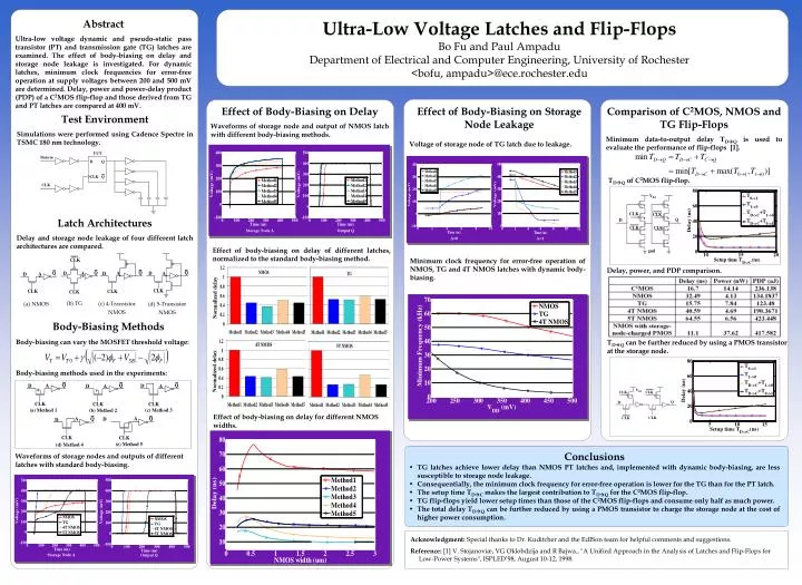
A=0 A=1 Storage Node A Output Q Storage Node A Output Q Abstract Ultra-low voltage dynamic and pseudo-static pass transistor (PT) and transmission gate (TG) latches are examined. The effect of body‑biasing on delay and storage node leakage is investigated. For dynamic latches, minimum clock frequencies for error-free operation at supply voltages between 200 and 500 mV are determined. Delay, power and power-delay product (PDP) of a C2MOS flip-flop and those derived from TG and PT latches are compared at 400 mV. Ultra-Low Voltage Latches and Flip-Flops Bo Fu and Paul Ampadu Department of Electrical and Computer Engineering, University of Rochester <bofu, ampadu>@ece.rochester.edu Effect of Body-Biasing on Delay Waveforms of storage node and output of NMOS latch with different body-biasing methods. Effect of Body-Biasing on Storage Node Leakage Comparison of C2MOS, NMOS and TG Flip-Flops Minimum data-to-output delay TDQ is used to evaluate the performance of flip-flops [1]. Test Environment Simulations were performed using Cadence Spectre in TSMC 180 nm technology. Voltage of storage node of TG latch due to leakage. TDQof C2MOS flip-flop. Latch Architectures Delay and storage node leakage of four different latch architectures are compared. Effect of body-biasing on delay of different latches, normalized to the standard body-biasing method. Minimum clock frequency for error-free operation of NMOS, TG and 4T NMOS latches with dynamic body-biasing. Delay, power, and PDP comparison. Normalized delay (b) TG (a) NMOS (c) 4-Transistor NMOS (d) 5-Transistor NMOS Body-Biasing Methods Body-biasing can vary the MOSFET threshold voltage: TDQcan be further reduced by using a PMOS transistor at the storage node. Normalized delay Body-biasing methods used in the experiments: Effect of body-biasing on delay for different NMOS widths. • Conclusions • TG latches achieve lower delay than NMOS PT latches and, implemented with dynamic body-biasing, are less susceptible to storage node leakage. • Consequentially, the minimum clock frequency for error-free operation is lower for the TG than for the PT latch. • The setup time TDC makes the largest contribution to TDQ for the C2MOS flip-flop. • TG flip-flops yield lower setup times than those of the C2MOS flip-flops and consume only half as much power. • The total delay TDQ can be further reduced by using a PMOS transistor to charge the storage node at the cost of higher power consumption. Waveforms of storage nodes and outputs of different latches with standard body-biasing. Acknowledgment: Special thanks to Dr. Kuditcher and the EdISon team for helpful comments and suggestions. Reference: [1] V. Stojanoviæ, VG Oklobdzija and R Bajwa., "A Unified Approach in the Analysis of Latches and Flip-Flops for Low-Power Systems", ISPLED’98, August 10-12, 1998.