Download
1 / 78
780 likes | 862 Vues
Single Cycle CPU. Questions on CS140 ? Computer Arithmetic ? Attend office hours with TAs or me. Do the exercises in the text. Previously: built and ALU. Today: Actually build a CPU. The Story so far:. Instruction Set Architectures Performance issues

E N D
Single Cycle CPU • Questions on CS140 ? • Computer Arithmetic ? • Attend office hours with TAs or me. • Do the exercises in the text. • Previously: built and ALU. • Today: Actually build a CPU Tarun Soni, Summer’03
The Story so far: • Instruction Set Architectures • Performance issues • 2s complement, Addition, Subtraction • Multiplication, Division, Floating Point numbers Basically ISA & ALU stuff Tarun Soni, Summer’03
CPU: Building blocks CarryIn • Adder • MUX • ALU A 32 Sum Adder 32 B Carry 32 Select A 32 MUX Y 32 B 32 OP A 32 Result ALU 32 B 32 Tarun Soni, Summer’03
CarryIn A[31..0] 32 32 Sum[31..0] Adder 32 Select B[31..0] Carry A 32 MUX Y A[63..32] CarryIn 32 32 B 32 Sum[63..32] Adder 32 OP B[63..32] Carry 32 CPU: Building blocks • Building a 64-bit adder from 2x32-bit adders Tarun Soni, Summer’03
CarryIn A[31..0] Sum[31..0] 32 Adder 32 Select B[31..0] Carry 32 A 32 MUX Sum[63..32] Cin=0 32 A[63..32] B 32 32 S Adder 32 B[63..32] Select Cout 32 Cin=1 A 1 A[63..32] MUX Cout 32 1 S B 32 Adder 1 B[63..32] Cout 32 CPU: Building blocks • Silicon is cheap – sort-of Tarun Soni, Summer’03
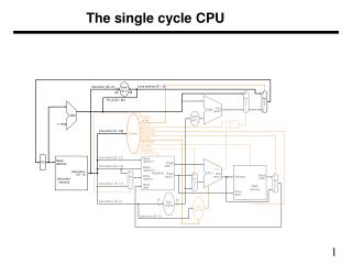
CPU Single Cycle CPU Tarun Soni, Summer’03
Control Datapath CPU The Big Picture: Where are We Now? • The Five Classic Components of a Computer • Datapath Design, then Control Design Processor Input Memory Output Tarun Soni, Summer’03
Instruction Fetch Instruction Decode Operand Fetch Execute Result Store Next Instruction CPU: The big picture Execute Decode Fetch Fetch Store Next Execute an entire instruction ° Design hardware for each of these steps!!! Tarun Soni, Summer’03
. . . . . . . . . . . . CPU: Clocking Clk Setup Hold Setup Hold Don’t Care • All storage elements are clocked by the same clock edge Tarun Soni, Summer’03
CPU The Big Picture: The Performance Perspective • Execution Time = Insts * CPI * Cycle Time • Processor design (datapath and control) will determine: • Clock cycle time • Clock cycles per instruction • Starting today: • Single cycle processor: • Advantage: One clock cycle per instruction • Disadvantage: long cycle time Execute an entire instruction Tarun Soni, Summer’03
CPI Inst. Count Cycle Time CPU • We're ready to look at an implementation of the MIPS • Simplified to contain only: • memory-reference instructions: lw, sw • arithmetic-logical instructions: add, sub, and, or, slt • control flow instructions: beq • Generic Implementation: • use the program counter (PC) to supply instruction address • get the instruction from memory • read registers • use the instruction to decide exactly what to do • All instructions use the ALU after reading the registers memory-reference? arithmetic? control flow? Tarun Soni, Summer’03
31 26 21 16 11 6 0 op rs rt rd shamt funct 6 bits 5 bits 5 bits 5 bits 5 bits 6 bits 31 26 21 16 0 immediate op rs rt 6 bits 5 bits 5 bits 16 bits 31 26 0 op target address 6 bits 26 bits CPU Review: The MIPS Instruction Formats • The different fields are: • op: operation of the instruction • rs, rt, rd: the source and destination register specifiers • shamt: shift amount • funct: selects the variant of the operation in the “op” field • address / immediate: address offset or immediate value • target address: target address of the jump instruction Tarun Soni, Summer’03
31 26 21 16 11 6 0 op rs rt rd shamt funct 6 bits 5 bits 5 bits 5 bits 5 bits 6 bits 31 26 21 16 0 op rs rt immediate 6 bits 5 bits 5 bits 16 bits 31 26 21 16 0 op rs rt displacement 6 bits 5 bits 5 bits 16 bits CPU • R-type • add rd, rs, rt • sub, and, or, slt • LOAD and STORE • lw rt, rs, imm16 • sw rt, rs, imm16 • BRANCH: • beq rs, rt, imm16 Tarun Soni, Summer’03
CPU Requirements to implement the ISA • Memory • instruction & data • Registers (32 x 32) • read RS • read RT • Write RT or RD • PC • Extender • Add and Sub register or extended immediate • Add 4 or extended immediate to PC Tarun Soni, Summer’03
CPU • Combinational Elements • Storage Elements • Clocking methodology A State Element C = f(A,B,state) {State[n] = f(A,B,state[n-1])} B clk A Combinational Logic C = f(A,B) B Tarun Soni, Summer’03
CPU: Storage unit • The set-reset latch • output depends on present inputs and also on past inputs Tarun Soni, Summer’03
CPU: D-flip flop • Two inputs: • the data value to be stored (D) • the clock signal (C) indicating when to read & store D • Two outputs: • the value of the internal state (Q) and it's complement • Output changes only on the clock edge Tarun Soni, Summer’03
CPU: Clocking Methodology • An edge triggered methodology • Typical execution: • read contents of some state elements, • send values through some combinational logic • write results to one or more state elements Tarun Soni, Summer’03
CPU: Storage block Write Enable • Register • Similar to the D Flip Flop except • N-bit input and output • Write Enable input • Write Enable: • 0: Data Out will not change • 1: Data Out will become Data In (on the clock edge) Data In Data Out N N Clk Tarun Soni, Summer’03
CPU: Register Files RW RA RB Write Enable 5 5 5 • Register File consists of (32) registers: • Two 32-bit output buses: • One 32-bit input bus: busW • Register is selected by: • RA selects the register to put on busA • RB selects the register to put on busB • RW selects the register to be writtenvia busW when Write Enable is 1 • Clock input (CLK) • Factor only during write-enable=1; • Otherwise, this unit acts just like combinational logic. busA busW 32 32 32-bit Registers 32 busB Clk 32 Tarun Soni, Summer’03
CPU: Register Files Still use the real clock (not shown here) to do the actual write Built using D-flip flops Tarun Soni, Summer’03
CPU: Memory Write Enable Address • Memory (idealized) • One input bus: Data In • One output bus: Data Out • Memory word is selected by: • Address selects the word to put on Data Out • Write Enable = 1: address selects the memoryword to be written via the Data In bus • Clock input (CLK) • The CLK input is a factor ONLY during write operation • During read operation, behaves as a combinational logic block: • Address valid => Data Out valid after “access time.” Data In DataOut 32 32 Clk Tarun Soni, Summer’03
CPU: RTL RegisterTransfer Language (RTL) • is a mechanism for describing the movement and manipulation of data between storage elements: • R[3] <- R[5] + R[7] • PC <- PC + 4 + R[5] • R[rd] <- R[rs] + R[rt] • R[rt] <- Mem[R[rs] + immed] Tarun Soni, Summer’03
CPU: More building blocks Tarun Soni, Summer’03
Instruction Fetch Instruction Decode Operand Fetch Execute Result Store Next Instruction CPU: The big picture Execute Decode Fetch Fetch Store Next Execute an entire instruction ° Design hardware for each of these steps!!! Tarun Soni, Summer’03
PC Clk Next Address Logic Address Instruction Memory CPU: Instruction Fetch • RTL version of the instruction fetch step: • Fetch the Instruction: mem[PC] • Update the program counter: • Sequential Code: PC <- PC + 4 • Branch and Jump: PC <- “something else” Instruction Word 32 Tarun Soni, Summer’03
CPU: Binary arithmetic for PC • In theory, the PC is a 32-bit byte address into the instruction memory: • Sequential operation: PC<31:0> = PC<31:0> + 4 • Branch operation: PC<31:0> = PC<31:0> + 4 + SignExt[Imm16] * 4 • The magic number “4” always comes up because: • The 32-bit PC is a byte address • And all our instructions are 4 bytes (32 bits) long • In other words: • The 2 LSBs of the 32-bit PC are always zeros • There is no reason to have hardware to keep the 2 LSBs • In practice, we can simplify the hardware by using a 30-bit PC<31:2>: • Sequential operation: PC<31:2> = PC<31:2> + 1 • Branch operation: PC<31:2> = PC<31:2> + 1 + SignExt[Imm16] • In either case: Instruction Memory Address = PC<31:2> concat “00” Tarun Soni, Summer’03
CPU: Instruction Fetch unit • The common RTL operations • Fetch the Instruction: inst <- mem[PC] • Update the program counter: • Sequential Code: PC <- PC + 4 • Branch and Jump PC <- “something else” Tarun Soni, Summer’03
31 26 21 16 11 6 0 op rs rt rd shamt funct 6 bits 5 bits 5 bits 5 bits 5 bits 6 bits CPU: Register-Register Operations (Add, Subtract etc.) • R[rd] <- R[rs] op R[rt] Example: addU rd, rs, rt • Ra, Rb, and Rw come from instruction’s rs, rt, and rd fields • ALUctr and RegWr: control logic after decoding the instruction Rd Rs Rt ALUctr RegWr 5 5 5 busA Rw Ra Rb busW 32 32 32-bit Registers Result ALU 32 32 busB Clk 32 ° Worry about instruction decode to generate ALUctr and RegWr later. Tarun Soni, Summer’03
CPU: Register - Register Timing Clk Clk-to-Q Old Value New Value PC Instruction Memory Access Time Rs, Rt, Rd, Op, Func Old Value New Value Delay through Control Logic ALUctr Old Value New Value RegWr Old Value New Value Register File Access Time busA, B Old Value New Value ALU Delay busW Old Value New Value Rd Rs Rt ALUctr Register Write Occurs Here RegWr 5 5 5 busA Rw Ra Rb busW 32 32 32-bit Registers Result ALU 32 32 busB Clk 32 Tarun Soni, Summer’03
11 31 26 21 16 0 op rs rt immediate 6 bits 5 bits 5 bits 16 bits rd? 31 16 15 0 immediate 0 0 0 0 0 0 0 0 0 0 0 0 0 0 0 0 16 bits 16 bits CPU: Logical Immediate Op. • R[rt] <- R[rs] op ZeroExt[imm16] ] Handle Rt as destination Rd Rt RegDst Mux Rs ALUctr RegWr 5 5 5 busA Rw Ra Rb busW 32 Result 32 32-bit Registers ALU 32 32 busB Clk 32 Mux Handle Immediate as operand ZeroExt imm16 32 16 ALUSrc Tarun Soni, Summer’03
11 31 26 21 16 0 op rs rt immediate 6 bits 5 bits 5 bits 16 bits rd CPU: Load Operations • R[rt] <- Mem[R[rs] + SignExt[imm16]] Example: lw rt, rs, imm16 Rd Rt Reg-Write could be from result or data memory Need data Memory! RegDst Mux Rs ALUctr RegWr 5 5 5 busA W_Src Rw Ra Rb busW 32 32 32-bit Registers ALU 32 32 busB Clk MemWr 32 Mux Mux WrEn Adr Data In 32 Data Memory 32 Extender imm16 32 16 Clk ALUSrc Tarun Soni, Summer’03 ExtOp
31 26 21 16 0 op rs rt immediate 6 bits 5 bits 5 bits 16 bits CPU: Store Operations • Mem[ R[rs] + SignExt[imm16] <- R[rt] ] Example: sw rt, rs, imm16 Reg can write to Data Memory Rd Rt ALUctr MemWr W_Src RegDst Mux Rs Rt RegWr 5 5 5 busA Rw Ra Rb busW 32 32 32-bit Registers ALU 32 32 busB Clk 32 Mux Mux WrEn Adr Data In 32 32 Data Memory Extender imm16 32 16 Clk Tarun Soni, Summer’03 ALUSrc ExtOp
31 26 21 16 0 op rs rt immediate 6 bits 5 bits 5 bits 16 bits CPU: Branching • beq rs, rt, imm16 • mem[PC] Fetch the instruction from memory • Equal <- R[rs] == R[rt] Calculate the branch condition • if (COND eq 0) Calculate the next instruction’s address • PC <- PC + 4 + ( SignExt(imm16) x 4 ) • else • PC <- PC + 4 Tarun Soni, Summer’03
31 26 21 16 0 op rs rt immediate 6 bits 5 bits 5 bits 16 bits Cond Rs Rt 4 RegWr 5 5 5 busA Adder Rw Ra Rb busW 32 32 32-bit Registers Equal? Mux PC busB Clk 32 Adder Clk CPU: Datapath for Branching • beq rs, rt, imm16 Datapath generates condition (equal) Inst Address nPC_sel 32 00 imm16 Calculate the “condition” part of the branch op. PC Ext Calculate (PC+4) as well as (imm16+PC+4) and choose one Tarun Soni, Summer’03
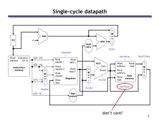
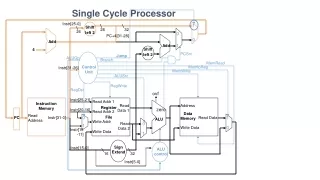
Inst Memory Adr Adder Mux Adder CPU: The Aggregate Datapath Instruction<31:0> <21:25> <16:20> <11:15> <0:15> Still need to worry about Instruction Decode Rs Rt Rd Imm16 RegDst nPC_sel ALUctr MemWr MemtoReg Equal Rt Rd 0 1 Rs Rt 4 RegWr 5 5 5 busA Rw Ra Rb = busW 00 32 32 32-bit Registers ALU 0 32 busB 32 0 PC 32 Mux Mux Clk 32 WrEn Adr 1 Clk 1 Data In Extender Data Memory imm16 PC Ext 32 16 imm16 Clk ExtOp ALUSrc Tarun Soni, Summer’03
ALU PC Clk CPU: Datapath: High-level view • Register file and ideal memory: • The CLK input is a factor ONLY during write operation • During read operation, behave as combinational logic: • Address valid => Output valid after “access time.” Critical Path (Load Operation) = PC’s Clk-to-Q + Instruction Memory’s Access Time + Register File’s Access Time + ALU to Perform a 32-bit Add + Data Memory Access Time + Setup Time for Register File Write + Clock Skew Ideal Instruction Memory Instruction Rd Rs Rt Imm 5 5 5 16 Instruction Address A Data Address 32 Rw Ra Rb 32 Ideal Data Memory 32 32 32-bit Registers Next Address Data In B Clk Clk 32 Tarun Soni, Summer’03
CPU: Control Signals Instruction<31:0> Inst Memory <21:25> <21:25> <16:20> <11:15> <0:15> Adr Op Fun Rt Rs Rd Imm16 Control ALUctr nPC_sel MemWr MemtoReg ALUSrc RegWr RegDst ExtOp Equal DATA PATH Tarun Soni, Summer’03
Inst Memory Adr Adder Mux Adder CPU: Control Signals: Meaning • Rs, Rt, Rd and Imed16 hardwired into datapath • nPC_sel: 0 => PC <– PC + 4; 1 => PC <– PC + 4 + SignExt(Im16) || 00 nPC_sel 4 00 PC Clk imm16 PC Ext Tarun Soni, Summer’03
CPU: Control Signals: Meaning • ExtOp: “zero”, “sign” • ALUsrc: 0 => regB; 1 => immed • ALUctr: “add”, “sub”, “or” • MemWr: write memory • MemtoReg: 1 => Mem • RegDst: 0 => “rt”; 1 => “rd” • RegWr: write dest register RegDst ALUctr MemWr MemtoReg Equal Rt Rd 0 1 Rs Rt RegWr 5 5 5 busA = Rw Ra Rb busW 32 32 32-bit Registers ALU 0 32 busB 32 0 32 Mux Mux Clk 32 WrEn Adr 1 1 Data In Data Memory imm16 Extender 32 16 Clk Tarun Soni, Summer’03 ExtOp ALUSrc
CPU: Control Signals for various operations inst Register Transfer ADD R[rd] <– R[rs] + R[rt]; PC <– PC + 4 ALUsrc = RegB, ALUctr = “add”, RegDst = rd, RegWr, nPC_sel = “+4” SUB R[rd] <– R[rs] – R[rt]; PC <– PC + 4 ALUsrc = RegB, ALUctr = “sub”, RegDst = rd, RegWr, nPC_sel = “+4” ORi R[rt] <– R[rs] + zero_ext(Imm16); PC <– PC + 4 ALUsrc = Im, Extop = “Z”, ALUctr = “or”, RegDst = rt, RegWr, nPC_sel = “+4” LOAD R[rt] <– MEM[ R[rs] + sign_ext(Imm16)]; PC <– PC + 4 ALUsrc = Im, Extop = “Sn”, ALUctr = “add”, MemtoReg, RegDst = rt, RegWr, nPC_sel = “+4” STORE MEM[ R[rs] + sign_ext(Imm16)] <– R[rs]; PC <– PC + 4 ALUsrc = Im, Extop = “Sn”, ALUctr = “add”, MemWr, nPC_sel = “+4” BEQ if ( R[rs] == R[rt] ) then PC <– PC + sign_ext(Imm16)] || 00 else PC <– PC + 4 nPC_sel = EQUAL, ALUctr = “sub” Tarun Soni, Summer’03
CPU: Control Signals: Logic Design • nPC_sel <= if (OP == BEQ) then EQUAL else 0 • ALUsrc <= if (OP == “000000”) then “regB” else “immed” • ALUctr <= if (OP == “000000”) then funct elseif (OP == ORi) then “OR” elseif (OP == BEQ) then “sub” else “add” • ExtOp <= _____________ • MemWr <= _____________ • MemtoReg <= _____________ • RegWr: <=_____________ • RegDst: <= _____________ Tarun Soni, Summer’03
CPU: Control Signals: Logic Design • nPC_sel <= if (OP == BEQ) then EQUAL else 0 • ALUsrc <= if (OP == “000000”) then “regB” else “immed” • ALUctr <= if (OP == “000000”) then funct elseif (OP == ORi) then “OR” elseif (OP == BEQ) then “sub” else “add” • ExtOp <= if (OP == ORi) then “zero” else “sign” • MemWr <= (OP == Store) • MemtoReg <= (OP == Load) • RegWr: <= if ((OP == Store) || (OP == BEQ)) then 0 else 1 • RegDst: <= if ((OP == Load) || (OP == ORi)) then 0 else 1 Tarun Soni, Summer’03
Instruction<31:0> Inst Memory <0:15> <21:25> <16:20> <11:15> Adr Rs Rt Rd Imm16 RegDst nPC_sel ALUctr MemWr MemtoReg Rt Equal Rd rt add +4 0 1 Rs Rt 4 RegWr 5 5 5 busA Adder Rw Ra Rb = busW 00 32 32 32-bit Registers ALU 0 32 Mux busB 32 0 PC 32 Mux Mux Clk 32 Adder WrEn Adr 1 Clk 1 Data In Data Memory Extender imm16 PC Ext 32 16 imm16 Clk sign ext ExtOp ALUSrc CPU: Example: Load R[rt] <- Mem[R[rs] + SignExt[imm16]] Viz., lw rt, rs, imm16 Tarun Soni, Summer’03
ALU PC Clk CPU: The abstract version Control Ideal Instruction Memory Control Signals Conditions Instruction Rd Rs Rt 5 5 5 Instruction Address A Data Address Data Out 32 Rw Ra Rb 32 Ideal Data Memory 32 32 32-bit Registers Next Address Data In B Clk Clk 32 Datapath • Logical vs. Physical Structure Tarun Soni, Summer’03
CPU: The real thing Tarun Soni, Summer’03
CPU: 5 steps to design • 5 steps to design a processor • 1. Analyze instruction set => datapath requirements • 2. Select set of datapath components & establish clock methodology • 3. Assemble datapath meeting the requirements • 4. Analyze implementation of each instruction to determine setting of control points that effects the register transfer. • 5. Assemble the control logic • MIPS makes it easier • Instructions same size • Source registers always in same place • Immediates same size, location • Operations always on registers/immediates • Single cycle datapath => CPI=1, CCT => long Tarun Soni, Summer’03
Processor Input Control Memory Datapath Output CPU: Control Section • The Five Classic Components of a Computer Tarun Soni, Summer’03
31 26 21 16 11 6 0 op rs rt rd shamt funct 6 bits 5 bits 5 bits 5 bits 5 bits 6 bits CPU: Add Instruction • add rd, rs, rt • mem[PC] Fetch the instruction from memory • R[rd] <- R[rs] + R[rt] The actual operation • PC <- PC + 4 Calculate the next instruction’s address Tarun Soni, Summer’03
Inst Memory Instruction<31:0> Adr nPC_sel 4 Adder 00 Mux PC Adder Clk imm16 CPU: The Add Instruction • Fetch the instruction from Instruction memory: Instruction <- mem[PC] • This is the same for all instructions Instruction Fetch Unit at the Beginning of Add PC Ext Tarun Soni, Summer’03