Download
1 / 14
140 likes | 310 Vues
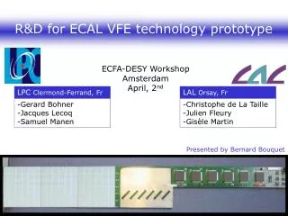
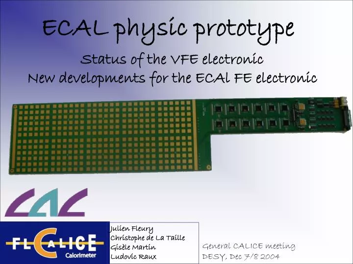
ECAL physic prototype. Status of the VFE electronic New developments for the ECAl FE electronic. Julien Fleury Christophe de La Taille Gisèle Martin Ludovic Raux. General CALICE meeting DESY, Dec 7/8 2004. Outline. Chip development. What could be a FE chip for the ECAL

E N D
ECAL physic prototype Status of the VFE electronic New developments for the ECAl FE electronic Julien Fleury Christophe de La Taille Gisèle Martin Ludovic Raux General CALICE meeting DESY, Dec 7/8 2004
Outline Chip development • What could be a FE chip for the ECAL • Test blocks for a FE chip • FLC_TECH : a first approach to a front-end chip • Embedding Front-end and A/D conversion PCB development • Expectations for the front-end PCB • Technology : state of the art • A new PCB towards final detector • PCB design, next step
Block scheme of a possible FE electronic Out Power control Channel Select Digital memory 6 Chan. 12 BCID ADC Energy 3 BCID Ch.2 Gain 1 100 10 Ch.36 Ch.1
Possible output block Format • Channel level auto-trigger Native zero suppress that reduce significantly the data flow • Serial output • To simplify as much as possible the FE to DAQ interface ADC result - 12 bit Channel nb - 6 bit BCID – 12 bit Chip ID - x bit Gain - 2 bit Position Energy Time
Test block : Characterisation of different architecture Designed block, many measurement results @LCWS2005 Preamplifier - Multi gain charge preamplifier with idle mode Shapers • Integration shaper, integration time 100ns, @LPC • Opamp shaper : conservative version, peaking time 200ns • Current feedback opamp, peaking time 200ns, Gain BW 2GHz • Capacom shaper, variable peaking time, variable gain ADC • Pipeline ADC, 10bit @LPC • SAR ADC, 10bit • Wilkinson ADC (slow structure), 12bit
FLC_TECH1 : a first step towards a FE electronic FLC_TECH description • -4 channels • Multi-gain charge preamplifier • 2 shaping : gain 1 and gain 10 • 5-depht SCA • Multiplexed output, auto-trigger and Idle mode Ch.1 1 SCA (depht : 5) 10 Output Multiplexing Ch.2 Ch.4 Chip OK Test board OK Meas. Results @ LCWS2005
next step : embedding front-end and A/D conversion • In 2005 : • Merging of LAL preamplifier and shaper with LPC shaper and ADC Study of on-chip A/D conversion 1 ADC 10 Output Input Shaper
Cooling VFE chip Si Wafers PCB Tungsten 8.5mm Expectations for a front-end PCB - As thin as possible, to reduce the molier radius - Small line capacitance from diode to FE chip, to reduce noise A solution : FE chip embedded in the detector Cut of a slab
Technology : state of the art Copper – 17.5µm Isolation Isolation 100 µm Multilayer PCB Multilayer PCB Single ended via hole (Cost 30% more than a normal PCB) PCB thickness = (Nb of layer-1)*100µm 6 layers 500µm To avoid to have via on the Wafer pads (risk of short with the glue)
A new PCB towards final detector 1mm 62 62mm Using FLC_PHY3 (No idle mode, external bias devices) • 2 active wafers • Compatible with ECAL physics proto • 8 temperature measurement • FE Chips on back of PCB • Designed for AC coupled wafers • Validation of epitaxial capacitance
PCB design : Next step After that step • Using of AC coupled wafers will be validated • Wafer process, gluing process • Main mechanical issues will be figured out • Heating will be measured (8 meas. Point inside the detector) Next step • A new PCB version will be designed when a new FE chip will be validated (digital output, 36 channels, idle mode) • Manpower will be focused on microelectronic R&D
Conclusion PCB design • A new PCB is currently in design • to validate the AC coupled wafers • to get used with detector embedded front-end chip It will be ready in february 2005 Chip design • Many blocks has been designed for a technologic prototype • Next couple of month will be spent to characterize them 2005 target : get an ADC in a FE chip.