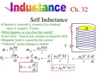
Download
1 / 91
920 likes | 1.15k Vues
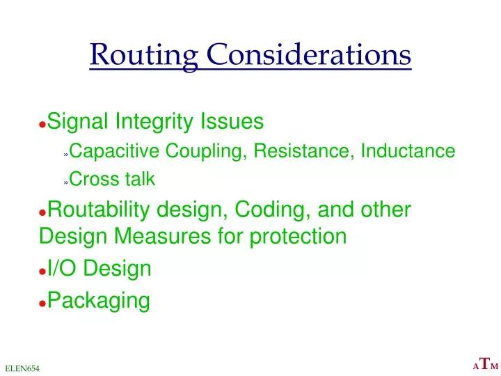
Routing Considerations. Signal Integrity Issues Capacitive Coupling, Resistance, Inductance Cross talk Routability design, Coding, and other Design Measures for protection I/O Design Packaging. Impact of Interconnect Parasitics. • Reduce Robustness. • Affect Performance Increase delay

E N D
Routing Considerations Signal Integrity Issues Capacitive Coupling, Resistance, Inductance Cross talk Routability design, Coding, and other Design Measures for protection I/O Design Packaging
Impact of Interconnect Parasitics • Reduce Robustness • • Affect Performance • Increase delay • Increase power dissipation Classes of Parasitics • Capacitive • Resistive • Inductive
Capacitive Cross TalkDynamic Node V DD CLK C XY Y C Y In 1 X In PDN 2 2.5 V In 3 0 V CLK 3 x 1 mm overlap: 0.19 V disturbance
Capacitive Cross TalkDriven Node 0.5 0.45 0.4 tr↑ X 0.35 C R XY 0.3 Y V Y tXY = RY(CXY+CY) X 0.25 C Y 0.2 V (Volt) 0.15 0.1 0.05 0 0 0.2 0.4 0.6 0.8 1 t (nsec) Keep time-constant smaller than rise time
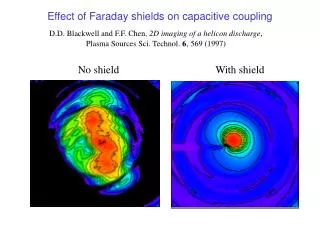
Dealing with Capacitive Cross Talk • Avoid floating nodes • Protect sensitive nodes • Make rise and fall times as large as possible • Differential signaling • Do not run wires together for a long distance • Use shielding wires • Use shielding layers
Shielding Shielding wire GND Shielding V DD layer GND Substrate ( GND )
Cross Talk and Performance -When neighboring lines switch in opposite direction of victim line, delay increases DELAY DEPENDENT UPON ACTIVITY IN NEIGHBORING WIRES Cc Miller Effect - Both terminals of capacitor are switched in opposite directions (0 Vdd, Vdd 0) - Effective voltage is doubled and additional charge is needed (from Q=CV)
Impact of Cross Talk on Delay r is ratio between capacitance to GND and to neighbor
Structured Predictable Interconnect • Example: Dense Wire Fabric ([Sunil Kathri]) • Trade-off: • Cross-coupling capacitance 40x lower, 2% delay variation • Increase in area and overall capacitance • Also: FPGAs, VPGAs
e Interconnect ProjectionsLow-k dielectrics • Both delay and power are reduced by dropping interconnect capacitance • Types of low-k materials include: inorganic (SiO2), organic (Polyimides) and aerogels (ultra low-k) • The numbers below are on the conservative side of the NRTS roadmap
Encoding Data Avoids Worst-CaseConditions In Encoder Bus Decoder Out
Interconnects Information Theoretic Approach to Address Delay and Reliability in Long On-chip Interconnects
Sources of Error on Interconnects • Capacitive Coupling • Inductive Coupling • Process Variations • Power Noise
Signal Integrity • Tradition: • Protect the signal on every single wire. • Design the clock period to be greater than the worst case delay. • Questions asked? • Is it an overkill? • Can some errors be tolerated? • Can this be optimized?
Capacitive Coupling • Signals are influenced by the signals in the adjacent wires due to coupling capacitance • Phenomenon known as “Crosstalk” • Results in “Deterministic” Delay Variations
Modeling Interconnects • O(s) = G(s).I(s) I(s) O(s) G(s)
Modeling Interconnects G(s) O(s) I(s) Structure Capacitive Coupling
Modeling Interconnects G(s) O(s) I(s) Structure Inductive Coupling
Modeling Interconnects G(s) O(s) I(s) Randomness Power Noise
Modeling Interconnects G(s) O(s) I(s) Randomness Process Variations
Transfer Function • O(s) = F(s).I(s) • F(s) = (1 + L(s)C(s))-1
Problems in Interconnects • Delay • Power • Reliability
Binary Symmetric Channel • Inputs, Outputs Є {0,1} • Crossover Probability pe 1-pe 0 0 pe pe 1 1 1-pe
Self Information(of an event) • Defined as • - log2(p) • p is the probability of occurrence. • Example • if 1 occurs with p = ½, then every time it occurs -log2(1/2) = 1 bits of information is conveyed.
Entropy • Entropy of a system of random events is the measure of uncertainty • Defined as • H(S)= -Σ p.log2(p) • p is the probability of occurrence of each event in the system. • Example: • For a random binary system • H = - p1.log2(p1) - p0.log2(p0) • If p1 = p0 = ½, H = 1 bit.
Conditional Entropy • The uncertainty in one system, given the outcome of the second system. • Defined as • H(S1|S2) = -Σ Σ pjk.log2(pjk/pk) • J and k are events in systems 1 and 2 respectively. • The equation represents the entropy of system1 conditioned upon the outcome of system 2.
Channel Capacity • reduction in uncertainty about the input given the output • C = H(Si) – H(Si|So) • For p1 = p0 = ½ • C = 1 + pe.log2(pe) + (1-pe).log2(1-pe)
Channels with memory • Have multiple states • A1, A2,…, An • Each state has a probability of occurrence • p1,p2,…,pn • Each state has a probability of error • pe1,pe2,…,pen • Capacity of each state • Ci = 1 + pei log(pei) + (1+pei) log(1+pei) • Capacity of channel • C=Σ pi Ci
Concluding Remark • Non of the simple ad-hoc codes are approaching the capacity • Current/Future work • Capacity-approaching bus codes.. and bus design
V DD V V in out C L Driving Large Capacitances • Transistor Sizing • Cascaded Buffers
Using Cascaded Buffers In Out CL = 20 pF 1 2 N 0.25 mm process Cin =2.5 fF tp0 = 30 ps F = CL/Cin = 8000 fopt = 3.6 N = 7 tp = 0.76 ns
Trade off Performance for Area and Energy Given tpmax find N and f Area Energy Output Driver Design
Delay as a Function of F and N 10,000 F 10,000 = 1000 tp/tp0 0 p t / p t 100 F 1000 = F 100 = 10 1 3 5 7 9 11 Number of buffer stages N
Output Driver Design 0.25 mm process, CL = 20 pF Transistor Sizes for optimally-sized cascaded buffer tp= 0.76 ns Transistor Sizes of redesigned cascaded buffer tp= 1.8 ns
How to Design Large Transistors D(rain) Reduces diffusion capacitance Reduces gate resistance Multiple Contacts S(ource) G(ate) small transistors in parallel
Bonding Pad Design Bonding Pad GND 100 mm Out VDD Out In GND
ESD Protection • When a chip is connected to a board, there is unknown (potentially large) static voltage difference • Equalizing potentials requires (large) charge flow through the pads • Diodes sink this charge into the substrate – need guard rings to pick it up.
ESD Protection Diode
Chip Packaging • Bond wires (~25m) are used to connect the package to the chip • Pads are arranged in a frame around the chip • Pads are relatively large (~100m in 0.25m technology),with large pitch (100m) • Many chips areas are ‘pad limited’