Download
1 / 53
720 likes | 1.23k Vues
High-Performance Schottky Barrier MOSFET. Horng-Chih Lin Department of Electronics Engineering & Institute of Electronics National Chiao Tung University September 19, 2005. Outline. Background Low B Source Field-induced Drain (FID) Structure Non-Si Channel Materials

E N D
High-Performance Schottky Barrier MOSFET Horng-Chih Lin Department of Electronics Engineering & Institute of Electronics National Chiao Tung University September 19, 2005
Outline • Background • Low BSource • Field-induced Drain (FID) Structure • Non-Si Channel Materials • Interface Modulation Techniques • Summary
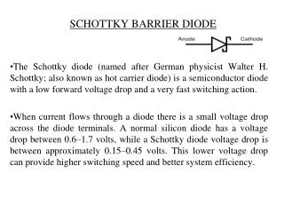
Gate Substrate SBMOSFET • Source/drain made of metallic material (e.g., silicide) in lieu of heavily doped semiconductor. • First reported in 1968 by Lepselter and Sze ( Proc. of IEEE, p.1400 (1968)). Source Drain Silicide
Advantages of SB MOSFET • Easy processing • Elimination of S/D implant • Ultra-shallow and abrupt junction • Low S/D sheet resistance • Low process temperature
ITRS 2003 Device Intrinsic Speed Ion:Ioff Ratio
Potential Distribution IEEE ED, V-47, p.1241 (2000) Source Source Channel Channel Drain Drain On-state (VG > VT) Off-state (VG < VT)
Major Issues (I) • On current, limited by • Barrier height • - PtSi (Bp = 0.24 eV) for pMOS • - ErSi2(Bn = 0.27 eV) for nMOS • - Near-zero or negative Bp desired • (ii) Barrier width • -Modulated by gate bias • - Gate overlaps with source • necessary bn
Major Issues (II) • Off current • Major Conduction mechanism: • Field emission of holes (electrons) for nMOS (pMOS) at drain junction • (ii) Structure • Gate/drain overlap structure aggravates the leakage bp
n+ poly: L = 27 nm; p+ poly: L = 40 nm Performance of Sub- 40 nm pMOSAppl. Phys. Lett., V-74, p.1174 (1999)
25nm p-Channel SOI SB MOSFET Jpn. J. Appl. Phys. (Part I), V-39, p.4757 (2000) • PtSi source/drain and metal gate
Methods to Improve Performance • Development of low BS/D materials • - Zero or even negative barrier height highly desired • - Use of SOI with ultra-thin body to reduce the leakage • Implementation of FID structure • Use of non-Si channel materials • - Exs. CNT and Ge (SiGe) channel • Metal/channel interface modulation • - Insertion of an ultra-thin dielectric layer • - Dopant segregation
Outline • Background • Low BSource • Field-induced Drain (FID) Structure • Non-Si Channel Materials • Interface Modulation Techniques • Summary
Barrier Height at Silicide/Si Junctions (1) IEDM Tech. Dig. p.57 (2000) (2) EDL., Vol.25, p.525 (2004)
Characteristics of Schottky Diodes EDL., Vol.25, p.525 (2004)
NMOS with YbSi2-x S/D IEEE EDL., Vol.25, p.525 (2004)
SB MOSFETs Built on SOI with Ultra-thin body VD VD Buried oxide Significant portion of the leakage blocked by the buried oxide
SB MOSFET on Ultra-thin Body SOIIEDM ‘2000, p.57 SOI thickness ~ 10 nm
Outline • Background • Low BS/D • Field-induced Drain (FID) Structure • Non-Si Channel Materials • Interface Modulation Techniques • Summary
Sub-gate Sub-gate Substrate Substrate SB MOSFETs with Field-induced Drain (FID) SA structure NSA structure
Sub-gate Substrate - Barrier width modulated by sub-gate bias - Source NOT necessary to overlap with the main-gate - Ambipolar operation capability
Fabrication Flow - Amorphous Si deposition (LPCVD, 550 oC, 50 nm) - Re-crystallization (in N2, 600 oC, 24 hr) - Gate oxide (LPCVD, 20 nm) - Gate formation (n+ poly-Si, 200 nm ) - CVD oxide (LPCVD, 200 nm) - Oxide patterning - Co salicide treatment
Fabrication Flow (Cont.) - Passivation (PECVD oxide, 550 nm) - Contact hole patterning - Metal pad and sub-gate formation
Sub-gate Source Drain VG << Vth Reduction of Off-state Leakage by FID • The FID expels the high-field region away from the drain junction. • Field-emission leakage encountered in conventional SB devices thus suppressed.
Sub-gate Modulation of ON Current by FID • Tunneling barrier width modulated by the sub-gate bias. • Depending on the polarity of applied bias, the device could be set for either n- or p-mode operation. Source VG > Vth Drain Dashed line has higher sub-gate bias
Ambipolar Poly-Si TFTs with FID H. C. Lin et al., IEDM’2000, p.857 Conventional SB TFT FID SB TFT VD = 5V VD = -5V Vsub=50V VD = 5V Vsub=-50V VD = -5V VG (V) -On/off current ratio ~ 106 • On/off current ratio < 103
10-8 10-9 ID(A) 10-10 10-11 @RT 10-12 -4 -3 -2 -1 0 VG (V) New Modified Characterization Scheme H. C. Lin et al., IEDM’2004, p.781 Step 1: Determination of VFB The new method Step 2:s as a function of VG Incremental method Step 3: Extract of DOS FEC theory Only two simple I-V measurements at room temperature from a single device are all that needed for full band-gap DOS extraction
Effect of Channel Crystallization SPC Channel, L/W = 1/20 mm/mm As-deposited SPC ELA
TEM Photos As-deposited poly-Si Grain size ~ 20 nm Grain size ~ 300 nm Grain size ~ 50 nm
VG n+ poly-Si gate Channel length VD VS Fin width CoSi2 source CoSi2 drain Al sub-gate VG, sub SB FinFET The top view of device structure SEM
Ambipolar Operation with Ideal Subthreshold Swing (IEEE NANO’02) VG,sub= 7.5 V VD = -1.5 V VD = 1.5 V VD = -0.1 V, VD = 0.1 V SS=60.8 mV/dec. SS= 60.6 mV/dec L = 470 nm, Fin width = 50 nm
Impact of S/D Material IEEE EDL., Vol.24, p.102 (2003) VG - Vth = 0 ~ -1.2 V in steps of - 0.2 V VG - Vth = 0 ~ -1.2 V in steps of - 0.2 V L = 110 nm PtSi S/D CoSi S/D
CNT Devices with FID IEDM’2004 p. 687
CNT Devices with FID IEDM’2004 p. 687
Outline • Background • Low BSource • Field-induced Drain (FID) Structure • Non-Si Channel Materials • Interface Modulation Techniques • Summary
SB MOSFET with SiGe Channel IEEE EDL Vol. 23, p. 460 (2002)
SB MOSFET with SiGe Channel IEEE EDL Vol. 23, p. 460 (2002)
Ge pMOSFETs With NiGe S/D IEEE EDL Vol. 26, p. 81 (2005) • NiGe S/D • Barrier height ~ 0.16 eV • Drive current 5 times higher than Si PMOS with PtSi S/D
SB PMOS on GOI with GePt S/D IEEE EDL Vol. 26, Vol. 26, p. 102 (2005)
CNT FET with Negative Barrier Height Nature, Vol.424, p.654 (2003) Bp of –0.05 eV was reported for CNT FET
Outline • Background • Low BSource • Field-induced Drain (FID) Structure • Non-Si Channel Materials • Interface Modulation Techniques • Summary
Reduction of Tunneling Resistance with an Ultrathin Interfacial Layer IEEE Trans. Nanotechnology, Vol.3 p.92 (2003) The Si in the direct vicinity of the metal acquires a dipole moment due to the influence of metal-induced gap states, generating a barrier to electron injection. An ultrathin insulator at the interface trades a reduction in the thermionic for a tunneling barrier. The key is to reduce the thermionic barrier while limiting the tunneling barrier.
Reduction of Tunneling Resistance with an Ultrathin Interfacial Layer IEEE Trans. Nanotechnology, Vol.3 p.92 (2003) Resistance drops sharply as gap states are blocked and the Fermi level is liberated.
Reduction of Tunneling Resistance with an Ultrathin Interfacial Layer IEEE Trans. Nanotechnology, Vol.3 p.92 (2003) Dependences of drain current and conductance on drain bias
Schottky Barrier Height Engineering with Dopant Segregation (DS) Technique (VLSI’04, p.168)
Schottky Barrier Height Engineering with Dopant Segregation (DS) Technique (VLSI’04, p.168)
+ BF2 SDE NiSi Si FinFET with Modified-Schottky Barrier (MSB) IEEE Electron Device Lett., Vol. 25, p.430 (2004)
Gate Ni silicide A A’ Lg=25 nm Source Drain Si FinFET with Modified-Schottky Barrier (MSB) IEEE Electron Device Lett., Vol. 25, p.430 (2004) Device Layout TEM
Si FinFET with Modified-Schottky Barrier (MSB) IEEE Electron Device Lett., Vol. 25, p.430 (2004)
Micro-structure of S/D in MSB FinFETs IEEE Electron Device Lett., Vol. 26, p.394 (2005) Fin width = 40 nm Fin width = 200 nm