Download
1 / 80
900 likes | 1.33k Vues
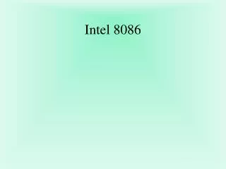
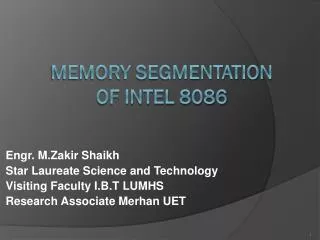
INTEL 8086. By: HAMDA ROZEEN 12BME15 NEMRA KANWAL 12BME24 UREEBA RAJPUT 12BME32. First 16- bit processor released by INTEL in the year 1978. Internal Architecture Of 8086. AX. IP. BX. Fetch & store code bytes in PIPELINE. CX. CS. DS. ES. SS. DX. CODE OUT.

E N D
By: HAMDA ROZEEN 12BME15 NEMRA KANWAL 12BME24 UREEBA RAJPUT 12BME32
AX IP BX Fetch & store code bytes in PIPELINE CX CS DS ES SS DX CODE OUT CODE IN IP BX DI PIPELINE (or) QUEUE DI SI EU BIU D E C O D E R SP BP Default Assignment Timing control ALU
The Architecture Of 8086 Includes: Arithematic Logic Unit (ALU) Flags General Registers Instruction Byte Queue Segment Registers 8086 Has Been Partitioned Into Two Functional Blocks: Execution Unit (EU) Bus Interface Unit (BIU)
The Execution Unit (EU) Has: Conrtol Unit. Instruction Decoder. Arithematic And Logical Unit (ALU). General Registers. Flag Register. Pointers. Index Registers. Execution unit contains the complete infrastructure required to execute an instruction. . . EU is responsible for executing the instructions of the programs and to carry out the required processing.
Control Unit Control unit is responsible for the co-ordination of all other units of the processor Instruction Decoder The instruction decoder translates the instructions fetched from the memory into a series of actions that are carried out by the EU Arithematic And Logical Unit (ALU) ALU performs various arithmetic and logical operations over the data
General Registers General registers are used for temporary storage and manipulation of data and instructions General Registers Are: Accumulator Register Base Register Count Register Data Register
Accumulator Register 16-bit register AX; 8-bit registers [AL+AH]. Accumulator can be used for I/O operations and string manipulation Base register 16-bit register BX; 8-bit registers [BL+BH]. BX register usually contains a data pointer used for based, based indexed or register indirect addressing. Count Register 16-bit register CX; 8-bit registers [CL+CH]. Count register can be used as a counter in string manipulation and shift/rotate instructions Data Register 16-bit register DX; 8-bit registers [DL+DH]. Data register can be used to hold 16 bit result in 32-bit operations.
Sign Carry Auxiliary Interrupt Zero Parity Trap Over flow Direction U - Unused • Flag Register (16-bit) • A flag is a flip flop which indicates some conditions produced by the execution of an instruction or controls certain operations of the EU. • 9 of the 16 are active flags and remaining 7 are undefined. • Active Flags; • 6 flags indicates some conditions- Status Flags • 3 flags –Control Flags
Status Flags Carry Flag (CF) - set if there was a carry from or borrow to the most significant bit during last result calculation Parity Flag (PF) - set if parity (the number of "1" bits) in the low-order byte of the result is even. Auxiliary Carry Flag (AF) - set if there was a carry from or borrow to bits 0-3 in the AL register. Zero Flag (ZF) - set if the result is zero. Sign Flag (SF) - set if the most significant bit of the result is one Overflow Flag (OF) - set if the size of the exceeds the capacity of the destination location.
Control Flags Single-step Flag (Trap F) – put 8086 in the single step mode Interrupt-enable Flag (IF) - setting this bit enables maskable interrupts . When IF=0, all maskable interrupt are disable Direction Flag (DF) – It is used with string operations. When set , it causing string instructions to auto – decrement or to process strings from right to left.
Pointers And Index Registers • Keep offset addresses • Used in various forms of memory addressing Stack Pointer (SP) is a 16-bit register pointing to program stack • Source Index (SI) is a 16-bit register. SI is used for indexed, based indexed and register indirect addressing, as well as a source data addresses in string manipulation instructions. • Base Pointer (BP) is a 16-bit register pointing to data in stack segment. BP register is usually used for based, based indexed or register indirect addressing. Destination Index (DI) is a 16-bit register. DI is used for indexed, based indexed and register indirect addressing, as well as a destination data addresses in string manipulation instructions.
The Bus Interface Unit (BIU) Has: 6-byte Instruction Queue The Segment Registers The Instruction Pointer The Address Summing Block The BIU handles all transactions of data and addresses on the buses for EU.
The Queue • The BIU uses a mechanism known as an instruction stream queue to implement a Pipeline Architecture. The queue permits pre-fetch of up to 6 bytes of instruction code. EU reads the instruction byte from the queue. These pre-fetching instructions are held in its FIFO queue. A byte is loaded at the input end of the queue, it automatically shifts up through the FIFO to the empty location nearest the output. The EU accesses the queue from the output end.
Physical Memory Segmented Memory 00000 • The total addressable memory size is 1MB • Most of the processor instructions use 16-bit pointers; the processor can effectively address only 64 KB of memory 1 MB • To access memory outside of 64 KB the CPU uses special Segment Registers to specify where the 64 KB segments are positioned within 1 MB of memory. FFFFF
Segment Registers Code Segment (CS) Register contains initial address of code segment with processor instructions. The processor uses CS for all accesses to instructions. Data Segment (DS) Register contain address of current data segment with program data. By default, the processor assumes that all data referenced by General Registers (AX, BX, CX, DX) and Index Register (SI, DI) is located in the Data Segment . Extra Segment (ES) Registercontains address of extra segment, usually with program data. By default, the processor assumes that the DI register references the ES in string manipulation instructions. Stack Segment (SS) Register contains address of stack segment with program stack. By default, the processor assumes that all data referenced by the Stack Pointer (SP) and Base Pointer (BP) registers is located in the Stack Segment.
Instruction Pointer And Summing Block Instruction Pointer contains 16-bit offset address of next instruction The value of the instruction pointer is incremented after executing every instruction. To form a 20bit address of the next instruction, the 16 bit address of the IP is added to the address contained in the CS , which has been shifted four bits to the left and this is done by the Summing Block.
8086 is designed to operate in two modes: Minimum Mode-- Single Processor. Maximum Mode-- Co-processor
AD0-AD15 (Bidirectional) Address/Data bus Low order address bus; these are multiplexed with data. When AD lines are used to transmit memory address the symbol A is used instead of AD, for example A0-A15. When data are transmitted over AD lines the symbol D is used in place of AD, for example D0-D7, D8-D15 or D0-D15.
A16/S3, A17/S4, A18/S5, A19/S6 Address/status High order address bus. These are multiplexed with status signals. When AS lines are used to transmit memory address the symbol A is used instead of As, for example A16-A19. S lines are indicating status signals. S3and S4indicates which segment register is being used. S5 updates interrupt enable flag at start of each cycle. S6 is always low.
BHE (Active Low)/S7 (Output) Bus High Enable/Status It is used to enable data onto the most significant half of data bus, D8-D15. 8-bit device connected to upper half of the data bus use BHE (Active Low) signal. It is multiplexed with status signal S7. MN/ MX MINIMUM / MAXIMUM This pin signal indicates what mode the processor is to operate in. RD (Read) (Active Low) The signal is used for read operation. It is an output signal. It is active when low.
Test Test input is tested by the ‘wait’ instruction. 8086 will enter a wait state after execution of the wait instruction and will resume execution only when the test is made low by an active hardware. This is used to synchronize an external activity to the processor internal operation READY This is the acknowledgement from the slow device or memory that they have completed the data transfer. The signal made available by the devices is synchronized by the 8284A clock generator to provide ready input to the 8086. The signal is active high.
RESET (Input) Causes the processor to immediately terminate its present activity. The signal must be active HIGH for at least four clock cycles. CLK The clock input provides the basic timing for processor operation and bus control activity. Its an asymmetric square wave with 33% duty cycle. INTR [Interrupt Request] This is a triggered input. This is sampled during the last clock cycles of each instruction to determine the availability of the request. If any interrupt request is pending, the processor enters the interrupt acknowledge cycle. This signal is active high and internally synchronized.
Hold Input signal to the processor from the bus masters as a request to grant the control of bus. Usually used by dma controller to get the control of the bus. Hlda Holdacknowledge Acknowledge signal by the processor to the bus master requesting the control of the bus through hold. The acknowledge is asserted high, when the processor accepts hold.
Rq/gt0 and rq /gt1 bus request/ bus grant These requests are used by other local bus masters to force the processor to release the local bus at the end of the processor’s current bus cycle. These pins are bidirectional. The request gt0 will have higher priority than gt1.
Wr Write control signal; asserted low whenever processor writes data to memory or i/o port. Lock an output signal activated by the lock prefix instruction. Remains active until the completion of the instruction prefixed by lock. The 8086 output low on the lock pin while executing an instruction prefixed by lock to prevent other bus masters from gaining control of the system bus.
m/io Used to differentiate memory access and i/o access. For memory reference instructions, it is high. For in and out instructions, it is low. Dt/r Data transmit/receive Output signal from the processor to control the direction of data flow through the data transceivers. Den Data enable Output signal from the processor used as output enable for the transceivers.
S0, s1, s2 Status signals Used by the 8086 bus controller to generate bus timing and control signals.
Ale Address latch enable Used to demultiplex the address and data lines using external latches. Inta Interrupt acknowledge When the interrupt request is accepted by the processor, the output is low on this line.
NMI NON-MASKABLE INTERRUPT: an edge triggered input which causes an interrupt request to the processor. A subroutine is vectored to via an interrupt vector lookup table located in system memory. NMI is not maskable internally by software. Qs0, qs1 Queue status The processor provides the status of queue in these lines. The queue status can be used by external device to track the internal status of the queue in 8086.
The set of mechanisms by which an instruction can specify how to obtain its operands is known as Addressing Modes. AddressingModes In 8086: 1. Register Addressing 2. Immediate Addressing 3. Direct Addressing Register Indirect Addressing Based Relative Addressing Indexed Relative Addressing Based Indexed Relative Addressing
Register Addressing Mode The operand to be accessed is specified as residing in an internal register. Example: MOV AX , BX Immediate Addressing Mode The operand is part of the instruction instead of the contents of a register or memory. Example: MOV AL , 015H
Direct Addressing Mode The operand is the combination of effective address and data segment register. It gives the physical address of the operand. Example: MOV CX , BETA Register Indirect Addressing Mode The operand is the combination of effective address and data segment register. The offset is specified, as effective address resides either in pointer register or index register. Example: MOV AX , [SI]
Based Addressing Mode The operand is the addition of direct or indirect displacement of contents of either Base Register or Base Pointer Register and value in DS and SS respectively. Example: MOV [BX] . BETA , AL Indexed Addressing Mode The operand is the addition of direct or indirect displacement of contents of IndexRegisters. Example MOV AL , ARRAY [SI]
Based Indexed Addressing Mode Combination of based addressing mode and the indexed addressing mode. Example: MOV AH , [BX] . BETA [SI]
The entire group of instructions that a microprocessor supports is called Instruction Set. 8086 has more than 20,000 instructions. Data Transfer Instructions Arithematic Instructions Bit Manipulation Instructions Program Execution Transfer Instructions String Instructions Process Control Instructions
MOV Des, Src: • Source operand can be register, memory location or immediate operand. • Destination can be register or memory operand. • Both Source and Destination cannot be memory location at the same time. • Example: • MOV CX, 037A H • MOV AL, BL • MOV BX, [0301 H]
PUSH Operand: • It pushes the operand into top of stack. • Example: • PUSH BX • POP Destination: • It pops the operand from top of stack to Destination. • Destination can be a general purpose register, segment register (except CS) or memory location. • Example: • POP AX
XCHG Des, Src: • This instruction exchanges Source with Destination. • It cannot exchange two memory locations directly. • Example: • XCHG DX, AX
IN Accumulator, Port Address: • It transfers the operand from specified port to accumulator register. • Example: • IN AX, 0028 H • OUT Port Address, Accumulator: • It transfers the operand from accumulator to specified port. • Example: • OUT 0028 H, AX
LEA Register, Src: • It loads a 16-bit register with the offset address of the data specified by the Source. • Example: • LEA BX, [DI]
LDS Des, Src: • It loads 32-bit pointer from memory source to destination register and DS. • The offset is placed in the destination register and the segment is placed in DS. • To use this instruction the word at the lower memory address must contain the offset and the word at the higher address must contain the segment. • Example: • LDS BX, [0301 H]