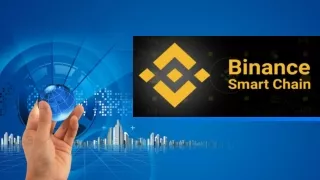
BINANCE SMART CHAIN DEVELOPMENT COMPANY IN NEW YORK
Binance Coin, the BNB coin address, wasnu2019t flexible, which led to the Binance smart chain Development Company. Both the blockchains operate side-by-side. Binance Smart Chain Development services is an independent blockchain that could run even if Binance Chain went offline. Binance Smart Chain Development is an independent blockchain that runs in tandem with the Binance Chain. It is built on Ethereum Virtual Machine (EVM), integrated with a robust smart contract. Due to which it is highly adaptable on a blockchain network. Binance Smart Chain isnu2019t a layer two or off-chain scalability solution, as it was pretended. Itu2019s an independent blockchain that could run even if Binance Chain went offline. Both the blockchains bear a strong resemblance from a design standpoint. As Binance Smart Chain is adaptable with Ethereum Virtual Machine, it proved beneficial for the users and the developers. For developers, it becomes easy to integrate their projects over Ethereum.Binance Coin, the BNB coin address, wasnu2019t flexible, which led to the Binance smart chain Development Company. Both the blockchains operate side-by-side. Binance Smart Chain Development services is an independent blockchain that could run even if Binance Chain went offline. Binance Smart Chain Development is an independent blockchain that runs in tandem with the Binance Chain. It is built on Ethereum Virtual Machine (EVM), integrated with a robust smart contract. Due to which it is highly adaptable on a blockchain network. Binance Smart Chain isnu2019t a layer two or off-chain scalability solution, as it was pretended. Itu2019s an independent blockchain that could run even if Binance Chain went offline. Both the blockchains bear a strong resemblance from a design standpoint. As Binance Smart Chain is adaptable with Ethereum Virtual Machine, it proved beneficial for the users and the developers. For developers, it becomes easy to integrate their projects over Ethereum.Binance Coin, the BNB coin address, wasnu2019t flexible, which led to the Binance smart chain Development Company. Both the blockchains operate side-by-side. Binance Smart Chain Development services is an independent blockchain that could run even if Binance Chain went offline. Binance Smart Chain Development is an independent blockchain that runs in tandem with the Binance Chain. It is built on Ethereum Virtual Machine (EVM), integrated with a robust smart contract. Due to which it is highly adaptable on a blockchain network. Binance Smart Chain isnu2019t a layer two or off-chain scalability solution, as it was pretended. Itu2019s an independent blockchain that could run even if Binance Chain went offline. Both the blockchains bear a strong resemblance from a design standpoint. As Binance Smart Chain is adaptable with Ethereum Virtual Machine, it proved beneficial for the users and the developers. For developers, it becomes easy to integrate their projects over Ethereum.Binance Coin, the BNB coin address, wasnu2019t flexible, which led to the Binance smart chain Development Company. Both the blockchains operate side-by-side. Binance Smart Chain Development services is an independent blockchain that could run even if Binance Chain went offline. Binance Smart Chain Development is an independent blockchain that runs in tandem with the Binance Chain. It is built on Ethereum Virtual Machine (EVM), integrated with a robust smart contract. Due to which it is highly adaptable on a blockchain network. Binance Smart Chain isnu2019t a layer two or off-chain scalability solution, as it was pretended. Itu2019s an independent blockchain that could run even if Binance Chain went offline. Both the blockchains bear a strong resemblance from a design standpoint. As Binance Smart Chain is adaptable with Ethereum Virtual Machine, it proved beneficial for the users and the developers. For developers, it becomes easy to integrate their projects over Ethereum.Binance Coin, the BNB coin address, wasnu2019t flexible, which led to the Binance smart chain Development Company. Both the blockchains operate side-by-side. Binance Smart Chain Development services is an independent blockchain that could run even if Binance Chain went offline. Binance Smart Chain Development is an independent blockchain that runs in tandem with the Binance Chain. It is built on Ethereum Virtual Machine (EVM), integrated with a robust smart contract. Due to which it is highly adaptable on a blockchain network. Binance Smart Chain isnu2019t a layer two or off-chain scalability solution, as it was pretended. Itu2019s an independent blockchain that could run even if Binance Chain went offline. Both the blockchains bear a strong resemblance from a design standpoint. As Binance Smart Chain is adaptable with Ethereum Virtual Machine, it proved beneficial for the users and the developers. For developers, it becomes easy to integrate their projects over Ethereum.Binance Coin, the BNB coin address, wasnu2019t flexible, which led to the Binance smart chain Development Company. Both the blockchains operate side-by-side. Binance Smart Chain Development services is an independent blockchain that could run even if Binance Chain went offline. Binance Smart Chain Development is an independent blockchain that runs in tandem with the Binance Chain. It is built on Ethereum Virtual Machine (EVM), integrated with a robust smart contract. Due to which it is highly adaptable on a blockchain network. Binance Smart Chain isnu2019t a layer two or off-chain scalability solution, as it was pretended. Itu2019s an independent blockchain that could run even if Binance Chain went offline. Both the blockchains bear a strong resemblance from a design standpoint. As Binance Smart Chain is adaptable with Ethereum Virtual Machine, it proved beneficial for the users and the developers. For developers, it becomes easy to integrate their projects over Ethereum.Binance Coin, the BNB coin address, wasnu2019t flexible, which led to the Binance smart chain Development Company. Both the blockchains operate side-by-side. Binance Smart Chain Development services is an independent blockchain that could run even if Binance Chain went offline. Binance Smart Chain Development is an independent blockchain that runs in tandem with the Binance Chain. It is built on Ethereum Virtual Machine (EVM), integrated with a robust smart contract. Due to which it is highly adaptable on a blockchain network. Binance Smart Chain isnu2019t a layer two or off-chain scalability solution, as it was pretended. Itu2019s an independent blockchain that could run even if Binance Chain went offline. Both the blockchains bear a strong resemblance from a design standpoint. As Binance Smart Chain is adaptable with Ethereum Virtual Machine, it proved beneficial for the users and the developers. For developers, it becomes easy to integrate their projects over Ethereum.Binance Coin, the BNB coin address, wasnu2019t flexible, which led to the Binance smart chain Development Company. Both the blockchains operate side-by-side. Binance Smart Chain Development services is an independent blockchain that could run even if Binance Chain went offline. Binance Smart Chain Development is an independent blockchain that runs in tandem with the Binance Chain. It is built on Ethereum Virtual Machine (EVM), integrated with a robust smart contract. Due to which it is highly adaptable on a blockchain network. Binance Smart Chain isnu2019t a layer two or off-chain scalability solution, as it was pretended. Itu2019s an independent blockchain that could run even if Binance Chain went offline. Both the blockchains bear a strong resemblance from a design standpoint. As Binance Smart Chain is adaptable with Ethereum Virtual Machine, it proved beneficial for the users and the developers. For developers, it becomes easy to integrate their projects over Ethereum.Binance Coin, the BNB coin address, wasnu2019t flexible, which led to the Binance smart chain Development Company. Both the blockchains operate side-by-side. Binance Smart Chain Development services is an independent blockchain that could run even if Binance Chain went offline. Binance Smart Chain Development is an independent blockchain that runs in tandem with the Binance Chain. It is built on Ethereum Virtual Machine (EVM), integrated with a robust smart contract. Due to which it is highly adaptable on a blockchain network. Binance Smart Chain isnu2019t a layer two or off-chain scalability solution, as it was pretended. Itu2019s an independent blockchain that could run even if Binance Chain went offline. Both the blockchains bear a strong resemblance from a design standpoint. As Binance Smart Chain is adaptable with Ethereum Virtual Machine, it proved beneficial for the users and the developers. For developers, it becomes easy to integrate their projects over Ethereum.Binance Coin, the BNB coin address, wasnu2019t flexible, which led to the Binance smart chain Development Company. Both the blockchains operate side-by-side. Binance Smart Chain Development services is an independent blockchain that could run even if Binance Chain went offline. Binance Smart Chain Development is an independent blockchain that runs in tandem with the Binance Chain. It is built on Ethereum Virtual Machine (EVM), integrated with a robust smart contract. Due to which it is highly adaptable on a blockchain network. Binance Smart Chain isnu2019t a layer two or off-chain scalability solution, as it was pretended. Itu2019s an independent blockchain that could run even if Binance Chain went offline. Both the blockchains bear a strong resemblance from a design standpoint. As Binance Smart Chain is adaptable with Ethereum Virtual Machine, it proved beneficial for the users and the developers. For developers, it becomes easy to integrate their projects over Ethereum.Binance Coin, the BNB coin address, wasnu2019t flexible, which led to the Binance smart chain Development Company. Both the blockchains operate side-by-side. Binance Smart Chain Development services is an independent blockchain that could run even if Binance Chain went offline. Binance Smart Chain Development is an independent blockchain that runs in tandem with the Binance Chain. It is built on Ethereum Virtual Machine (EVM), integrated with a robust smart contract. Due to which it is highly adaptable on a blockchain network. Binance Smart Chain isnu2019t a layer two or off-chain scalability solution, as it was pretended. Itu2019s an independent blockchain that could run even if Binance Chain went offline. Both the blockchains bear a strong resemblance from a design standpoint. As Binance Smart Chain is adaptable with Ethereum Virtual Machine, it proved beneficial for the users and the developers. For developers, it becomes easy to integrate their projects over Ethereum.Binance Coin, the BNB coin address, wasnu2019t flexible, which led to the Binance smart chain Development Company. Both the blockchains operate side-by-side. Binance Smart Chain Development services is an independent blockchain that could run even if Binance Chain went offline. Binance Smart Chain Development is an independent blockchain that runs in tandem with the Binance Chain. It is built on Ethereum Virtual Machine (EVM), integrated with a robust smart contract. Due to which it is highly adaptable on a blockchain network. Binance Smart Chain isnu2019t a layer two or off-chain scalability solution, as it was pretended. Itu2019s an independent blockchain that could run even if Binance Chain went offline. Both the blockchains bear a strong resemblance from a design standpoint. As Binance Smart Chain is adaptable with Ethereum Virtual Machine, it proved beneficial for the users and the developers. For developers, it becomes easy to integrate their projects over Ethereum.Binance Coin, the BNB coin address, wasnu2019t flexible, which led to the Binance smart chain Development Company. Both the blockchains operate side-by-side. Binance Smart Chain Development services is an independent blockchain that could run even if Binance Chain went offline. Binance Smart Chain Development is an independent blockchain that runs in tandem with the Binance Chain. It is built on Ethereum Virtual Machine (EVM), integrated with a robust smart contract. Due to which it is highly adaptable on a blockchain network. Binance Smart Chain isnu2019t a layer two or off-chain scalability solution, as it was pretended. Itu2019s an independent blockchain that could run even if Binance Chain went offline. Both the blockchains bear a strong resemblance from a design standpoint. As Binance Smart Chain is adaptable with Ethereum Virtual Machine, it proved beneficial for the users and the developers. For developers, it becomes easy to integrate their projects over Ethereum.Binance Coin, the BNB coin address, wasnu2019t flexible, which led to the Binance smart chain Development Company. Both the blockchains operate side-by-side. Binance Smart Chain Development services is an independent blockchain that could run even if Binance Chain went offline. Binance Smart Chain Development is an independent blockchain that runs in tandem with the Binance Chain. It is built on Ethereum Virtual Machine (EVM), integrated with a robust smart contract. Due to which it is highly adaptable on a blockchain network. Binance Smart Chain isnu2019t a layer two or off-chain scalability solution, as it was pretended. Itu2019s an independent blockchain that could run even if Binance Chain went offline. Both the blockchains bear a strong resemblance from a design standpoint. As Binance Smart Chain is adaptable with Ethereum Virtual Machine, it proved beneficial for the users and the developers. For developers, it becomes easy to integrate their projects over Ethereum.Binance Coin, the BNB coin address, wasnu2019t flexible, which led to the Binance smart chain Development Company. Both the blockchains operate side-by-side. Binance Smart Chain Development services is an independent blockchain that could run even if Binance Chain went offline. Binance Smart Chain Development is an independent blockchain that runs in tandem with the Binance Chain. It is built on Ethereum Virtual Machine (EVM), integrated with a robust smart contract. Due to which it is highly adaptable on a blockchain network. Binance Smart Chain isnu2019t a layer two or off-chain scalability solution, as it was pretended. Itu2019s an independent blockchain that could run even if Binance Chain went offline. Both the blockchains bear a strong resemblance from a design standpoint. As Binance Smart Chain is adaptable with Ethereum Virtual Machine, it proved beneficial for the users and the developers. For developers, it becomes easy to integrate their projects over Ethereum.Binance Coin, the BNB coin address, wasnu2019t flexible, which led to the Binance smart chain Development Company. Both the blockchains operate side-by-side. Binance Smart Chain Development services is an independent blockchain that could run even if Binance Chain went offline. Binance Smart Chain Development is an independent blockchain that runs in tandem with the Binance Chain. It is built on Ethereum Virtual Machine (EVM), integrated with a robust smart contract. Due to which it is highly adaptable on a blockchain network. Binance Smart Chain isnu2019t a layer two or off-chain scalability solution, as it was pretended. Itu2019s an independent blockchain that could run even if Binance Chain went offline. Both the blockchains bear a strong resemblance from a design standpoint. As Binance Smart Chain is adaptable with Ethereum Virtual Machine, it proved beneficial for the users and the developers. For developers, it becomes easy to integrate their projects over Ethereum.Binance Coin, the BNB coin address, wasnu2019t flexible, which led to the Binance smart chain Development Company. Both the blockchains operate side-by-side. Binance Smart Chain Development services is an independent blockchain that could run even if Binance Chain went offline. Binance Smart Chain Development is an independent blockchain that runs in tandem with the Binance Chain. It is built on Ethereum Virtual Machine (EVM), integrated with a robust smart contract. Due to which it is highly adaptable on a blockchain network. Binance Smart Chain isnu2019t a layer two or off-chain scalability solution, as it was pretended. Itu2019s an independent blockchain that could run even if Binance Chain went offline. Both the blockchains bear a strong resemblance from a design standpoint. As Binance Smart Chain is adaptable with Ethereum Virtual Machine, it proved beneficial for the users and the developers. For developers, it becomes easy to integrate their projects over Ethereum.Binance Coin, the BNB coin address, wasnu2019t flexible, which led to the Binance smart chain Development Company. Both the blockchains operate side-by-side. Binance Smart Chain Development services is an independent blockchain that could run even if Binance Chain went offline. Binance Smart Chain Development is an independent blockchain that runs in tandem with the Binance Chain. It is built on Ethereum Virtual Machine (EVM), integrated with a robust smart contract. Due to which it is highly adaptable on a blockchain network. Binance Smart Chain isnu2019t a layer two or off-chain scalability solution, as it was pretended. Itu2019s an independent blockchain that could run even if Binance Chain went offline. Both the blockchains bear a strong resemblance from a design standpoint. As Binance Smart Chain is adaptable with Ethereum Virtual Machine, it proved beneficial for the users and the developers. For developers, it becomes easy to integrate their projects over Ethereum.Binance Coin, the BNB coin address, wasnu2019t flexible, which led to the Binance smart chain Development Company. Both the blockchains operate side-by-side. Binance Smart Chain Development services is an independent blockchain that could run even if Binance Chain went offline. Binance Smart Chain Development is an independent blockchain that runs in tandem with the Binance Chain. It is built on Ethereum Virtual Machine (EVM), integrated with a robust smart contract. Due to which it is highly adaptable on a blockchain network. Binance Smart Chain isnu2019t a layer two or off-chain scalability solution, as it was pretended. Itu2019s an independent blockchain that could run even if Binance Chain went offline. Both the blockchains bear a strong resemblance from a design standpoint. As Binance Smart Chain is adaptable with Ethereum Virtual Machine, it proved beneficial for the users and the developers. For developers, it becomes easy to integrate their projects over Ethereum.Binance Coin, the BNB coin address, wasnu2019t flexible, which led to the Binance smart chain Development Company. Both the blockchains operate side-by-side. Binance Smart Chain Development services is an independent blockchain that could run even if Binance Chain went offline. Binance Smart Chain Development is an independent blockchain that runs in tandem with the Binance Chain. It is built on Ethereum Virtual Machine (EVM), integrated with a robust smart contract. Due to which it is highly adaptable on a blockchain network. Binance Smart Chain isnu2019t a layer two or off-chain scalability solution, as it was pretended. Itu2019s an independent blockchain that could run even if Binance Chain went offline. Both the blockchains bear a strong resemblance from a design standpoint. As Binance Smart Chain is adaptable with Ethereum Virtual Machine, it proved beneficial for the users and the developers. For developers, it becomes easy to integrate their projects over Ethereum.Binance Coin, the BNB coin address, wasnu2019t flexible, which led to the Binance smart chain Development Company. Both the blockchains operate side-by-side. Binance Smart Chain Development services is an independent blockchain that could run even if Binance Chain went offline. Binance Smart Chain Development is an independent blockchain that runs in tandem with the Binance Chain. It is built on Ethereum Virtual Machine (EVM), integrated with a robust smart contract. Due to which it is highly adaptable on a blockchain network. Binance Smart Chain isnu2019t a layer two or off-chain scalability solution, as it was pretended. Itu2019s an independent blockchain that could run even if Binance Chain went offline. Both the blockchains bear a strong resemblance from a design standpoint. As Binance Smart Chain is adaptable with Ethereum Virtual Machine, it proved beneficial for the users and the developers. For developers, it becomes easy to integrate their projects over Ethereum.Binance Coin, the BNB coin address, wasnu2019t flexible, which led to the Binance smart chain Development Company. Both the blockchains operate side-by-side. Binance Smart Chain Development services is an independent blockchain that could run even if Binance Chain went offline. Binance Smart Chain Development is an independent blockchain that runs in tandem with the Binance Chain. It is built on Ethereum Virtual Machine (EVM), integrated with a robust smart contract. Due to which it is highly adaptable on a blockchain network. Binance Smart Chain isnu2019t a layer two or off-chain scalability solution, as it was pretended. Itu2019s an independent blockchain that could run even if Binance Chain went offline. Both the blockchains bear a strong resemblance from a design standpoint. As Binance Smart Chain is adaptable with Ethereum Virtual Machine, it proved beneficial for the users and the developers. For developers, it becomes easy to integrate their projects over Ethereum.Binance Coin, the BNB coin address, wasnu2019t flexible, which led to the Binance smart chain Development Company. Both the blockchains operate side-by-side. Binance Smart Chain Development services is an independent blockchain that could run even if Binance Chain went offline. Binance Smart Chain Development is an independent blockchain that runs in tandem with the Binance Chain. It is built on Ethereum Virtual Machine (EVM), integrated with a robust smart contract. Due to which it is highly adaptable on a blockchain network. Binance Smart Chain isnu2019t a layer two or off-chain scalability solution, as it was pretended. Itu2019s an independent blockchain that could run even if Binance Chain went offline. Both the blockchains bear a strong resemblance from a design standpoint. As Binance Smart Chain is adaptable with Ethereum Virtual Machine, it proved beneficial for the users and the developers. For developers, it becomes easy to integrate their projects over Ethereum.Binance Coin, the BNB coin address, wasnu2019t flexible, which led to the Binance smart chain Development Company. Both the blockchains operate side-by-side. Binance Smart Chain Development services is an independent blockchain that could run even if Binance Chain went offline. Binance Smart Chain Development is an independent blockchain that runs in tandem with the Binance Chain. It is built on Ethereum Virtual Machine (EVM), integrated with a robust smart contract. Due to which it is highly adaptable on a blockchain network. Binance Smart Chain isnu2019t a layer two or off-chain scalability solution, as it was pretended. Itu2019s an independent blockchain that could run even if Binance Chain went offline. Both the blockchains bear a strong resemblance from a design standpoint. As Binance Smart Chain is adaptable with Ethereum Virtual Machine, it proved beneficial for the users and the developers. For developers, it becomes easy to integrate their projects over Ethereum.Binance Coin, the BNB coin address, wasnu2019t flexible, which led to the Binance smart chain Development Company. Both the blockchains operate side-by-side. Binance Smart Chain Development services is an independent blockchain that could run even if Binance Chain went offline. Binance Smart Chain Development is an independent blockchain that runs in tandem with the Binance Chain. It is built on Ethereum Virtual Machine (EVM), integrated with a robust smart contract. Due to which it is highly adaptable on a blockchain network. Binance Smart Chain isnu2019t a layer two or off-chain scalability solution, as it was pretended. Itu2019s an independent blockchain that could run even if Binance Chain went offline. Both the blockchains bear a strong resemblance from a design standpoint. As Binance Smart Chain is adaptable with Ethereum Virtual Machine, it proved beneficial for the users and the developers. For developers, it becomes easy to integrate their projects over Ethereum.Binance Coin, the BNB coin address, wasnu2019t flexible, which led to the Binance smart chain Development Company. Both the blockchains operate side-by-side. Binance Smart Chain Development services is an independent blockchain that could run even if Binance Chain went offline. Binance Smart Chain Development is an independent blockchain that runs in tandem with the Binance Chain. It is built on Ethereum Virtual Machine (EVM), integrated with a robust smart contract. Due to which it is highly adaptable on a blockchain network. Binance Smart Chain isnu2019t a layer two or off-chain scalability solution, as it was pretended. Itu2019s an independent blockchain that could run even if Binance Chain went offline. Both the blockchains bear a strong resemblance from a design standpoint. As Binance Smart Chain is adaptable with Ethereum Virtual Machine, it proved beneficial for the users and the developers. For developers, it becomes easy to integrate their projects over Ethereum.Binance Coin, the BNB coin address, wasnu2019t flexible, which led to the Binance smart chain Development Company. Both the blockchains operate side-by-side. Binance Smart Chain Development services is an independent blockchain that could run even if Binance Chain went offline. Binance Smart Chain Development is an independent blockchain that runs in tandem with the Binance Chain. It is built on Ethereum Virtual Machine (EVM), integrated with a robust smart contract. Due to which it is highly adaptable on a blockchain network. Binance Smart Chain isnu2019t a layer two or off-chain scalability solution, as it was pretended. Itu2019s an independent blockchain that could run even if Binance Chain went offline. Both the blockchains bear a strong resemblance from a design standpoint. As Binance Smart Chain is adaptable with Ethereum Virtual Machine, it proved beneficial for the users and the developers. For developers, it becomes easy to integrate their projects over Ethereum.Binance Coin, the BNB coin address, wasnu2019t flexible, which led to the Binance smart chain Development Company. Both the blockchains operate side-by-side. Binance Smart Chain Development services is an independent blockchain that could run even if Binance Chain went offline. Binance Smart Chain Development is an independent blockchain that runs in tandem with the Binance Chain. It is built on Ethereum Virtual Machine (EVM), integrated with a robust smart contract. Due to which it is highly adaptable on a blockchain network. Binance Smart Chain isnu2019t a layer two or off-chain scalability solution, as it was pretended. Itu2019s an independent blockchain that could run even if Binance Chain went offline. Both the blockchains bear a strong resemblance from a design standpoint. As Binance Smart Chain is adaptable with Ethereum Virtual Machine, it proved beneficial for the users and the developers. For developers, it becomes easy to integrate their projects over Ethereum.Binance Coin, the BNB coin address, wasnu2019t flexible, which led to the Binance smart chain Development Company. Both the blockchains operate side-by-side. Binance Smart Chain Development services is an independent blockchain that could run even if Binance Chain went offline. Binance Smart Chain Development is an independent blockchain that runs in tandem with the Binance Chain. It is built on Ethereum Virtual Machine (EVM), integrated with a robust smart contract. Due to which it is highly adaptable on a blockchain network. Binance Smart Chain isnu2019t a layer two or off-chain scalability solution, as it was pretended. Itu2019s an independent blockchain that could run even if Binance Chain went offline. Both the blockchains bear a strong resemblance from a design standpoint. As Binance Smart Chain is adaptable with Ethereum Virtual Machine, it proved beneficial for the users and the developers. For developers, it becomes easy to integrate their projects over Ethereum.Binance Coin, the BNB coin address, wasnu2019t flexible, which led to the Binance smart chain Development Company. Both the blockchains operate side-by-side. Binance Smart Chain Development services is an independent blockchain that could run even if Binance Chain went offline. Binance Smart Chain Development is an independent blockchain that runs in tandem with the Binance Chain. It is built on Ethereum Virtual Machine (EVM), integrated with a robust smart contract. Due to which it is highly adaptable on a blockchain network. Binance Smart Chain isnu2019t a layer two or off-chain scalability solution, as it was pretended. Itu2019s an independent blockchain that could run even if Binance Chain went offline. Both the blockchains bear a strong resemblance from a design standpoint. As Binance Smart Chain is adaptable with Ethereum Virtual Machine, it proved beneficial for the users and the developers. For developers, it becomes easy to integrate their projects over Ethereum.Binance Coin, the BNB coin address, wasnu2019t flexible, which led to the Binance smart chain Development Company. Both the blockchains operate side-by-side. Binance Smart Chain Development services is an independent blockchain that could run even if Binance Chain went offline. Binance Smart Chain Development is an independent blockchain that runs in tandem with the Binance Chain. It is built on Ethereum Virtual Machine (EVM), integrated with a robust smart contract. Due to which it is highly adaptable on a blockchain network. Binance Smart Chain isnu2019t a layer two or off-chain scalability solution, as it was pretended. Itu2019s an independent blockchain that could run even if Binance Chain went offline. Both the blockchains bear a strong resemblance from a design standpoint. As Binance Smart Chain is adaptable with Ethereum Virtual Machine, it proved beneficial for the users and the developers. For developers, it becomes easy to integrate their projects over Ethereum.Binance Coin, the BNB coin address, wasnu2019t flexible, which led to the Binance smart chain Development Company. Both the blockchains operate side-by-side. Binance Smart Chain Development services is an independent blockchain that could run even if Binance Chain went offline. Binance Smart Chain Development is an independent blockchain that runs in tandem with the Binance Chain. It is built on Ethereum Virtual Machine (EVM), integrated with a robust smart contract. Due to which it is highly adaptable on a blockchain network. Binance Smart Chain isnu2019t a layer two or off-chain scalability solution, as it was pretended. Itu2019s an independent blockchain that could run even if Binance Chain went offline. Both the blockchains bear a strong resemblance from a design standpoint. As Binance Smart Chain is adaptable with Ethereum Virtual Machine, it proved beneficial for the users and the developers. For developers, it becomes easy to integrate their projects over Ethereum.Binance Coin, the BNB coin address, wasnu2019t flexible, which led to the Binance smart chain Development Company. Both the blockchains operate side-by-side. Binance Smart Chain Development services is an independent blockchain that could run even if Binance Chain went offline. Binance Smart Chain Development is an independent blockchain that runs in tandem with the Binance Chain. It is built on Ethereum Virtual Machine (EVM), integrated with a robust smart contract. Due to which it is highly adaptable on a blockchain network. Binance Smart Chain isnu2019t a layer two or off-chain scalability solution, as it was pretended. Itu2019s an independent blockchain that could run even if Binance Chain went offline. Both the blockchains bear a strong resemblance from a design standpoint. As Binance Smart Chain is adaptable with Ethereum Virtual Machine, it proved beneficial for the users and the developers. For developers, it becomes easy to integrate their projects over Ethereum.Binance Coin, the BNB coin address, wasnu2019t flexible, which led to the Binance smart chain Development Company. Both the blockchains operate side-by-side. Binance Smart Chain Development services is an independent blockchain that could run even if Binance Chain went offline. Binance Smart Chain Development is an independent blockchain that runs in tandem with the Binance Chain. It is built on Ethereum Virtual Machine (EVM), integrated with a robust smart contract. Due to which it is highly adaptable on a blockchain network. Binance Smart Chain isnu2019t a layer two or off-chain scalability solution, as it was pretended. Itu2019s an independent blockchain that could run even if Binance Chain went offline. Both the blockchains bear a strong resemblance from a design standpoint. As Binance Smart Chain is adaptable with Ethereum Virtual Machine, it proved beneficial for the users and the developers. For developers, it becomes easy to integrate their projects over Ethereum.Binance Coin, the BNB coin address, wasnu2019t flexible, which led to the Binance smart chain Development Company. Both the blockchains operate side-by-side. Binance Smart Chain Development services is an independent blockchain that could run even if Binance Chain went offline. Binance Smart Chain Development is an independent blockchain that runs in tandem with the Binance Chain. It is built on Ethereum Virtual Machine (EVM), integrated with a robust smart contract. Due to which it is highly adaptable on a blockchain network. Binance Smart Chain isnu2019t a layer two or off-chain scalability solution, as it was pretended. Itu2019s an independent blockchain that could run even if Binance Chain went offline. Both the blockchains bear a strong resemblance from a design standpoint. As Binance Smart Chain is adaptable with Ethereum Virtual Machine, it proved beneficial for the users and the developers. For developers, it becomes easy to integrate their projects over Ethereum.Binance Coin, the BNB coin address, wasnu2019t flexible, which led to the Binance smart chain Development Company. Both the blockchains operate side-by-side. Binance Smart Chain Development services is an independent blockchain that could run even if Binance Chain went offline. Binance Smart Chain Development is an independent blockchain that runs in tandem with the Binance Chain. It is built on Ethereum Virtual Machine (EVM), integrated with a robust smart contract. Due to which it is highly adaptable on a blockchain network. Binance Smart Chain isnu2019t a layer two or off-chain scalability solution, as it was pretended. Itu2019s an independent blockchain that could run even if Binance Chain went offline. Both the blockchains bear a strong resemblance from a design standpoint. As Binance Smart Chain is adaptable with Ethereum Virtual Machine, it proved beneficial for the users and the developers. For developers, it becomes easy to integrate their projects over Ethereum.Binance Coin, the BNB coin address, wasnu2019t flexible, which led to the Binance smart chain Development Company. Both the blockchains operate side-by-side. Binance Smart Chain Development services is an independent blockchain that could run even if Binance Chain went offline. Binance Smart Chain Development is an independent blockchain that runs in tandem with the Binance Chain. It is built on Ethereum Virtual Machine (EVM), integrated with a robust smart contract. Due to which it is highly adaptable on a blockchain network. Binance Smart Chain isnu2019t a layer two or off-chain scalability solution, as it was pretended. Itu2019s an independent blockchain that could run even if Binance Chain went offline. Both the blockchains bear a strong resemblance from a design standpoint. As Binance Smart Chain is adaptable with Ethereum Virtual Machine, it proved beneficial for the users and the developers. For developers, it becomes easy to integrate their projects over Ethereum.Binance Coin, the BNB coin address, wasnu2019t flexible, which led to the Binance smart chain Development Company. Both the blockchains operate side-by-side. Binance Smart Chain Development services is an independent blockchain that could run even if Binance Chain went offline. Binance Smart Chain Development is an independent blockchain that runs in tandem with the Binance Chain. It is built on Ethereum Virtual Machine (EVM), integrated with a robust smart contract. Due to which it is highly adaptable on a blockchain network. Binance Smart Chain isnu2019t a layer two or off-chain scalability solution, as it was pretended. Itu2019s an independent blockchain that could run even if Binance Chain went offline. Both the blockchains bear a strong resemblance from a design standpoint. As Binance Smart Chain is adaptable with Ethereum Virtual Machine, it proved beneficial for the users and the developers. For developers, it becomes easy to integrate their projects over Ethereum.Binance Coin, the BNB coin address, wasnu2019t flexible, which led to the Binance smart chain Development Company. Both the blockchains operate side-by-side. Binance Smart Chain Development services is an independent blockchain that could run even if Binance Chain went offline. Binance Smart Chain Development is an independent blockchain that runs in tandem with the Binance Chain. It is built on Ethereum Virtual Machine (EVM), integrated with a robust smart contract. Due to which it is highly adaptable on a blockchain network. Binance Smart Chain isnu2019t a layer two or off-chain scalability solution, as it was pretended. Itu2019s an independent blockchain that could run even if Binance Chain went offline. Both the blockchains bear a strong resemblance from a design standpoint. As Binance Smart Chain is adaptable with Ethereum Virtual Machine, it proved beneficial for the users and the developers. For developers, it becomes easy to integrate their projects over Ethereum.Binance Coin, the BNB coin address, wasnu2019t flexible, which led to the Binance smart chain Development Company. Both the blockchains operate side-by-side. Binance Smart Chain Development services is an independent blockchain that could run even if Binance Chain went offline. Binance Smart Chain Development is an independent blockchain that runs in tandem with the Binance Chain. It is built on Ethereum Virtual Machine (EVM), integrated with a robust smart contract. Due to which it is highly adaptable on a blockchain network. Binance Smart Chain isnu2019t a layer two or off-chain scalability solution, as it was pretended. Itu2019s an independent blockchain that could run even if Binance Chain went offline. Both the blockchains bear a strong resemblance from a design standpoint. As Binance Smart Chain is adaptable with Ethereum Virtual Machine, it proved beneficial for the users and the developers. For developers, it becomes easy to integrate their projects over Ethereum.Binance Coin, the BNB coin address, wasnu2019t flexible, which led to the Binance smart chain Development Company. Both the blockchains operate side-by-side. Binance Smart Chain Development services is an independent blockchain that could run even if Binance Chain went offline. Binance Smart Chain Development is an independent blockchain that runs in tandem with the Binance Chain. It is built on Ethereum Virtual Machine (EVM), integrated with a robust smart contract. Due to which it is highly adaptable on a blockchain network. Binance Smart Chain isnu2019t a layer two or off-chain scalability solution, as it was pretended. Itu2019s an independent blockchain that could run even if Binance Chain went offline. Both the blockchains bear a strong resemblance from a design standpoint. As Binance Smart Chain is adaptable with Ethereum Virtual Machine, it proved beneficial for the users and the developers. For developers, it becomes easy to integrate their projects over Ethereum.Binance Coin, the BNB coin address, wasnu2019t flexible, which led to the Binance smart chain Development Company. Both the blockchains operate side-by-side. Binance Smart Chain Development services is an independent blockchain that could run even if Binance Chain went offline. Binance Smart Chain Development is an independent blockchain that runs in tandem with the Binance Chain. It is built on Ethereum Virtual Machine (EVM), integrated with a robust smart contract. Due to which it is highly adaptable on a blockchain network. Binance Smart Chain isnu2019t a layer two or off-chain scalability solution, as it was pretended. Itu2019s an independent blockchain that could run even if Binance Chain went offline. Both the blockchains bear a strong resemblance from a design standpoint. As Binance Smart Chain is adaptable with Ethereum Virtual Machine, it proved beneficial for the users and the developers. For developers, it becomes easy to integrate their projects over Ethereum.Binance Coin, the BNB coin address, wasnu2019t flexible, which led to the Binance smart chain Development Company. Both the blockchains operate side-by-side. Binance Smart Chain Development services is an independent blockchain that could run even if Binance Chain went offline. Binance Smart Chain Development is an independent blockchain that runs in tandem with the Binance Chain. It is built on Ethereum Virtual Machine (EVM), integrated with a robust smart contract. Due to which it is highly adaptable on a blockchain network. Binance Smart Chain isnu2019t a layer two or off-chain scalability solution, as it was pretended. Itu2019s an independent blockchain that could run even if Binance Chain went offline. Both the blockchains bear a strong resemblance from a design standpoint. As Binance Smart Chain is adaptable with Ethereum Virtual Machine, it proved beneficial for the users and the developers. For developers, it becomes easy to integrate their projects over Ethereum.Binance Coin, the BNB coin address, wasnu2019t flexible, which led to the Binance smart chain Development Company. Both the blockchains operate side-by-side. Binance Smart Chain Development services is an independent blockchain that could run even if Binance Chain went offline. Binance Smart Chain Development is an independent blockchain that runs in tandem with the Binance Chain. It is built on Ethereum Virtual Machine (EVM), integrated with a robust smart contract. Due to which it is highly adaptable on a blockchain network. Binance Smart Chain isnu2019t a layer two or off-chain scalability solution, as it was pretended. Itu2019s an independent blockchain that could run even if Binance Chain went offline. Both the blockchains bear a strong resemblance from a design standpoint. As Binance Smart Chain is adaptable with Ethereum Virtual Machine, it proved beneficial for the users and the developers. For developers, it becomes easy to integrate their projects over Ethereum.Binance Coin, the BNB coin address, wasnu2019t flexible, which led to the Binance smart chain Development Company. Both the blockchains operate side-by-side. Binance Smart Chain Development services is an independent blockchain that could run even if Binance Chain went offline. Binance Smart Chain Development is an independent blockchain that runs in tandem with the Binance Chain. It is built on Ethereum Virtual Machine (EVM), integrated with a robust smart contract. Due to which it is highly adaptable on a blockchain network. Binance Smart Chain isnu2019t a layer two or off-chain scalability solution, as it was pretended. Itu2019s an independent blockchain that could run even if Binance Chain went offline. Both the blockchains bear a strong resemblance from a design standpoint. As Binance Smart Chain is adaptable with Ethereum Virtual Machine, it proved beneficial for the users and the developers. For developers, it becomes easy to integrate their projects over Ethereum.Binance Coin, the BNB coin address, wasnu2019t flexible, which led to the Binance smart chain Development Company. Both the blockchains operate side-by-side. Binance Smart Chain Development services is an independent blockchain that could run even if Binance Chain went offline. Binance Smart Chain Development is an independent blockchain that runs in tandem with the Binance Chain. It is built on Ethereum Virtual Machine (EVM), integrated with a robust smart contract. Due to which it is highly adaptable on a blockchain network. Binance Smart Chain isnu2019t a layer two or off-chain scalability solution, as it was pretended. Itu2019s an independent blockchain that could run even if Binance Chain went offline. Both the blockchains bear a strong resemblance from a design standpoint. As Binance Smart Chain is adaptable with Ethereum Virtual Machine, it proved beneficial for the users and the developers. For developers, it becomes easy to integrate their projects over Ethereum.
66 views • 5 slides