Chapter 10 Etching
Chapter 10 Etching. Introduction to etching. Wet chemical etching: isotropic. Anisotropic etching of crystalline Si. Dry etching overview. Plasma etching mechanism. Types of plasma etch system. Dry etching issues. Dry etching method for various films.


Chapter 10 Etching
E N D
Presentation Transcript
Chapter 10 Etching • Introduction to etching. • Wet chemical etching: isotropic. • Anisotropic etching of crystalline Si. • Dry etching overview. • Plasma etching mechanism. • Types of plasma etch system. • Dry etching issues. • Dry etching method for various films. • Deep Si etching (can etch through a wafer). NE 343: Microfabrication and thin film technology Instructor: Bo Cui, ECE, University of Waterloo; http://ece.uwaterloo.ca/~bcui/ Textbook: Silicon VLSI Technology by Plummer, Deal and Griffin
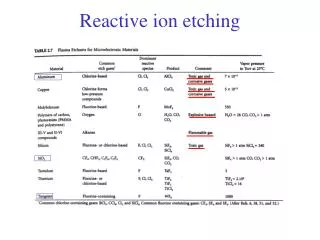
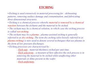
Material removal: etching processes • Etching is done either in “dry” or “wet” methods: • Wet etching uses liquid etchants with wafers immersed in etchant solution. • Wet etch is cheap and simple, but hard to control (not reproducible), not popular for nanofabrication for pattern transfer purpose. • Dry etch uses gas phase etchants in plasma, both chemical and physical (sputtering process). • Dry plasma etch works for many dielectric materials and some metals (Al, Ti, Cr, Ta, W…). • For other metals, ion milling (Ar+) can be used, but with low etching selectivity. (as a result, for metals that cannot be dry-etched, it is better to pattern them using liftoff) • Etching is consisted of 3 processes: • Mass transport of reactants (through a boundary layer) to the surface to be etched. • Reaction between reactants and the film to be etched at the surface. • Mass transport of reaction products from the surface through the surface boundary layer. Figures of merit: etch rate, etch rate uniformity, selectivity, and anisotropy.
Figures of merit: selectivity • Etching selectivity: • The ratio of etching rate between different materials, usually the higher the better. • Generally, chemical etching has high selectivity, physical etching (sputtering, milling) has low selectivity. • For fabrication, the selectivity is usually between film material and mask material, and is defined by Sfm. (f: film; m: mask) Temperature affects selectivity Etching with mask erosion
Selective over-etch of different materials The film is etched through to the bottom, plus over-etch to etch laterally for under-cut profile.
Figures of merit: anisotropy Isotropic: etch rate is the same along all directions. Anisotropic: etch rate depends on direction, usually vertical vs. horizontal. For isotropic, RI=1. For complete anisotropic, RI=0. CD: critical dimension
Figures of merit: anisotropy • Generally speaking, chemical process (wet etch, plasma etch) leads to isotropic etch; whereas physical process (directional energetic bombardment) leads to anisotropic etch. • Isotropic: • Best to use with large features when sidewall slope does not matter, and to undercut the mask (for easy liftoff). • Large critical dimension (CD, i.e. feature size) loss, generally not for nano-fabrication. • Quick, easy, and cheap. • Anisotropic: • Best for making small features with vertical sidewalls, preferred pattern transfer method for nano-fabrication and some micro-fabrication. • Typically more costly.
Chapter 10 Etching • Introduction to etching. • Wet chemical etching: isotropic. • Anisotropic etching of crystalline Si. • Dry etching overview. • Plasma etching mechanism. • Types of plasma etch system. • Dry etching issues. • Dry etching method for various films. • Deep Si etching (can etch through a wafer). NE 343: Microfabrication and Thin Film Technology Instructor: Bo Cui, ECE, University of Waterloo, bcui@uwaterloo.ca Textbook: Silicon VLSI Technology by Plummer, Deal, Griffin
Wet etching • Wet etching was used exclusively till 1970’s when feature size >3um. • For small scale features, large etch bias leads to significant CD (critical dimension) loss. • For today’s IC industry, wet etching is used for noncritical feature sizes. • Advantages: high selectivity, relatively inexpensive equipment, batch system with high throughput, etch rate can be very fast (many μm/min). • Disadvantages: generally isotropic profile, high chemical usage, poor process control (not so reproducible), excessive particulate contamination. • The etch rate can be controlled by any of the three serial processes: reactants transport to the surface (depends on chemical concentration and stirring…), reaction rate (depends on temperature), reaction products transport from the surface (depends on stirring…). • Preference is to have reaction rate controlled process because • Etch rate can be increased by temperature • Good control over reaction rate – temperature of a liquid is easy to control • Mass transport control will result in non-uniform etch rate: edge etches faster. • Etchant is often stirred to minimize boundary layer and make etching more uniform.
Isotropic wet etching (silicon dioxide) SiO2 etch rate SiO2 + 6HF H2SiF6+2H2O • Etch is isotropic and easily controlled by dilution of HF in H2O. • Thermally grown oxide etches at • 120nm/min in 6H2O:1HF • 1 m/min in 49 wt% HF (i.e. undiluted as purchased HF). • Faster etch rate for doped or deposited oxide. • High etch selectivity (SiO2/Si) > 100 • Buffered HF (BHF) or buffered oxide etchant (BOE) provides consistent etch rate • In regular HF etches, HF is consumed and the etch rate drops. • HF buffered with NH4F to maintain HF concentration, typically 6NH4F : 1HF • NH4F→NH3↑+ HF • HF is very dangerous! Because: • It is not a so strong acid (you don’t feel the pain for diluted HF). • Deceptive: it looks just like water. • It penetrates skin and attacks slowly the flesh and the bone. • It might be too late when you begin to feel the pain.
Isotropic etch (silicon) • Silicon is etched by nitric acid and hydrofluoric acid mixtures (HNO3 may be replaced by other strong oxidants like H2O2) • HNO3 partially decomposes to NO2, which oxidizes the surface of Si. • The HF then dissolves the SiO2. The overall reaction is: • Excess nitric acid results in a lot of silicon dioxide formation and etch rate becomes limited by HF removal of oxide (polishing). • CH3COOH (acetic acid) or H2O can be added as diluent, but etch differently. • Acetic acid is preferred because it prevents HNO3 dissociation. Si + 2NO2 + 2H2O SiO2 + H2 + 2HNO2 Si + HNO3 + 6HF → H2SiF6 + HNO2 + H2O + H2
Si iso-etch curves Regions exist where the reduction reaction is so slow, the surface is very planar and ends up being “polished” after the etch. Etch rate (m/min), VERY fast 1 2 As-purchased HF is 49.23%, and HNO3 69.51%) Region 1: High HF concentrations, reaction limited by HNO3, follow constant HNO3% lines. Rate limited by oxidation, etched wafer surface have some oxide. Region 2: High HNO3 concentrations, reaction limited by HF, follow constant HF % lines. Rate limited by reduction, etched wafer surface have more oxide.
Isotropic etching (aluminum) 50H3PO4 : 20H2O : 1HNO3 : 1CH3COOH Al3+ is water-soluble • Aluminum etches in water, phosphoric, nitric and acetic acid mixtures. • Converts Al to Al2O3with nitric acid (evolves H2). • Dissolve Al2O3 in phosphoric acid. • Gas evolution leading to bubbles. • Local etch rate goes down where bubble is formed, leading to non-uniformity. • Al can also be etched in (diluted) acid or base, such as HCl, HNO3, H2SO4, NaOH or KOH, but less controllable (etch the native oxide slowly and un-controllably, then once oxide all etched away, etch Al metal very fast). • The etch seems more repeatable in diluted HF (1:100 diluted), if one doesn’t bother to mix the above mixture (50H3PO4…).
Summary M: metal; PR: photoresist; Hac: acetic acid Those are just starting point, can use different ratios. E.g. the ratio for the Al etchant is different from previous slide. In addition, most metals can be etched by (diluted) acid, except Ti and Cr that form a dense stable oxide on top. Ti can be etched by HF; Cr by ceric ammonium nitrate plus acid.
Chapter 10 Etching • Introduction to etching. • Wet chemical etching: isotropic. • Anisotropic etching of crystalline Si. • Dry etching overview. • Plasma etching mechanism. • Types of plasma etch system. • Dry etching issues. • Dry etching method for various films. • Deep Si etching (can etch through a wafer). NE 343: Microfabrication and Thin Film Technology Instructor: Bo Cui, ECE, University of Waterloo, bcui@uwaterloo.ca Textbook: Silicon VLSI Technology by Plummer, Deal, Griffin
An-isotropic wet etching of Si: overview • Orientation selective etch of silicon occur in hydroxide solutions partly because of the closer packing of some orientations relative to other orientations • Density of planes: <111> > <110>, <100> • Etch rate: R(111) << R(110), R(100) • <100> direction etches faster than <111> direction, with etch rate • R(100) = few 100 R(111) • It is reaction rate limited • Used very widely in MEMS (micro electro mechanical systems), since it is inexpensive, fast etching and easy to control. {100} and {110} have 2 bonds below surface & 2 dangling bonds that can react. {111} plane has three of its bonds below surface & only one dangling bond to react → much slower etch rate.
An-isotropic wet etching of Si KOH etch example: 250 g KOH: 200 g 2-propanol, 800 g H2O at 80oC 1000 nm/min of [100] Etch stops at p++ layers Selectivity: {111}:{110}:{100} 1:600:400 KOH etching of <100> Si, 30% KOH solution Seidel’s etching model: Si + 2OH- Si(OH)22+ + 2e- Si(OH)22+ + 2OH- Si(OH)4 + 2e- Si(OH)4 + 4e- + 4H2O Si(OH)62- + 2H2 This is a model, real reaction is complicated. Si(OH)4is soluble. H2 is generated and form bubbles. m/hour temperature EDP: see later slides
Examples: for (100) wafer Effect of slow {111} etching with KOH: etching virtually stops at {111} plane. Etched trench Etch mask: SiO2 or Si3N4 or Cr/Au Etching selectivity to thermal oxide 1000, to LPCVD nitride infinity (>104!). But KOH attacks PECVD oxide and nitride. (100) Silicon wafer Etch “stops” at (111) direction
Examples: for (100) wafer Have been used to make bubble-jet printer nozzle.
AFM (atomic force microscope) tips (100) wafer For (110) (not (100)) wafer, vertical (not tapered) trench possible. What is the direction along the grating lines?
Other anisotropic silicon etchants • Tetramethyl Ammonium Hydroxide (TMAH) • Used widely as positive photoresist developer (since it contains no metal like K or Na, which are harmful for device.) • Typical etching at 80-90oC. • Etching rate 0.5-1.5 μm/min (10-40%w.t) • Selectivity <100> : <111> 10 - 35, much lower than KOH. • Result in rough surface(H2 bubble), KOH etch is smoother. • Like KOH, attacks aluminum • Like KOH, can use boron-stop-etching technique (etching rate decreases 40 times for 1020/cm3 boron doping). • Excellent selectivity of <100>Si : oxide/nitride (1: 5000-50000) • Ethylene DiaminePyrochatechol (EDP) • Typical etching temperature 115oC. • Etching rate 1μm/min. • Selectivity of <100>Si : oxide/nitride 3000-7000. • Doesn’t attack metal (Au, Cr, Cu, Ta) but attacks Al. • Selectivity <100> : <111> 35; (100) etches faster than (110), ((110) etches faster for KOH). • Excellent for boron stop technique, etching rate drops 50 times for 7x10¹⁹/cm3 boron doping. • Carcinogenic. http://en.wikipedia.org/wiki/Ethylenediamine_pyrocatechol
Etch stop • In wet etching process, etching depth is hard to control, so need etch stop layer. • Besides oxide and nitride, etching may be stopped by the following two methods, both related to doping of the silicon substrates. • Controlled by doping: doped Si dissolved slower than pure Si. • Controlled by electrochemical etch stop. Etch rate Boron concentration 5m x Etching stop by boron doping Boron concentration 1019 - 1020 Heavily doped boron layer (5-10m) mask Etching direction x
Electrochemical etch stop • When silicon is biased with a sufficiently large anodic potential relative to the etchant, it get oxidized due to electrochemical passivation, which then prevents etching. • For passivation to occur, current flow is required. • So if current flow can be prevented, there will be no oxide growth and etching can proceed. • Current flow can be prevented by adding a reverse-biased diode structure. When n-type exposed to solution, oxide forms and etch stops.