
Unit-1_
E N D
Presentation Transcript
ELECTRONIC SYSTEM AND PCB DESIGN(21ECC101J )Unit-1 DR. AARTI Sharma Assistant professor Department of Ece SRM IST, Delhi ncr campus
Course outcome of Unit-1 • At the end of this unit student will get to know about the basics of semiconductors and semiconductor devices.
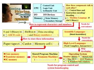
Contents • Classifications of Semiconductor • Doping in Semiconductors • Conductivity of semiconductors • Energy Distribution and fermi level • Carrier Concentration in intrinsic semiconductor and Mass-Action Law • Drift and Diffusion Current • Einstein Relationship for semiconductors
Intrinsicsemiconductors • An intrinsic semiconductor is one which is made of the semiconductor material in its extremely pure form. Examples : Si, Ge • The energy gap is so small that even at ordinary room temperature; there are many electrons which possess sufficient energy to jump across the small energy gap between the valence and the conduction bands. • Alternatively, an intrinsic semiconductor may be defined as one in which the number of conduction electrons is equal to the number of holes.
Fermi Energy and Fermi Level • Fermi Energy It is the maximum energy possessed by free electron at absolute zero temperature. • Fermi level It is the highest energy state occupied by free electron at absolute zero temperature.
Conductivity of Semiconductor Where σ is the conductivity of the semiconductor.
Fermi Dirac Function • Fermi Dirac Distribution is the probability distribution function which states the probability of finding an electron in the given energy level.
Carrier Concentration in Intrinsic semiconductor • In Intrinsic semiconductor when the valence electron broke covalent bond and jump into conduction band two types of charge carriers are generated. They are electrons and holes. Intrinsic carrier concentration • The number of electron per unit volume in conduction band or number of holes per unit volume in valence band is called intrinsic carrier concentration.
Drift Current • The current flow in semiconductor under the influence of electric field is called drift current.
Diffusion Current • The current flow in semiconductor from region of higher concentration to the lower concentration is called diffusion current.
Einstein Relationship • The equation which relates the mobility and the diffusion constant is known as Einstein relationship.
Advantages of Dual Gate MOSFET 1) Reduced channel and gate leakage current at off state which saves power. 2) Separate gate control on voltage saves power and chip area.
Challenges in Dual Gate MOSFET 1) Identically sized gates 2) Self alignment of source and drain to both gates 3) Alignment of both gates to each other 4) Connecting two gates with low resistance path
Applications of Dual Gate MOSFET 1) Mixers 2) Demodulators 3) Cascade amplifiers 4) Radio Frequency (RF) amplifier 5) Automatic Gain Control (AGC) amplifier
Fin FET .


![1_(1)[1]](https://cdn2.slideserve.com/5026441/slide1-dt.jpg)