Electronics Overview
Electronics Overview Electronics System Overview Power Backplane Readout Module (RM) Clock and Control Module (CCM) Calibration Module Theresa Shaw (FNAL) FE/DAQ Readout RBX Design Critical for Electonics RBX Provides Power, Cooling, Clock distribution, and

Electronics Overview
E N D
Presentation Transcript
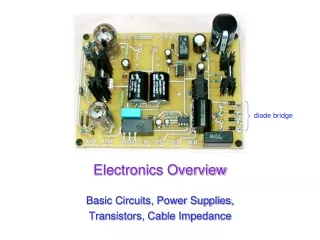
Electronics Overview • Electronics • System Overview • Power • Backplane • Readout Module (RM) • Clock and Control Module (CCM) • Calibration Module • Theresa Shaw • (FNAL)
RBX Design Critical for Electonics • RBX • Provides Power, • Cooling, • Clock distribution, and • Slow Controls Communication • RBX Design critical for • Connector Choice • Backplane development • Power/Grounding plans • Prototype Work this Summer
HB RBX • 36 HB RBXs 4968 Channels
HE Box • 36 HE RBXs 3672 Channels
Power Consumption • Power Consumption • HB RBX – 298 W HE RBX – 205 W 23A@6.5V 17A@6.5V • 33A@4.5V 21A@4.5V
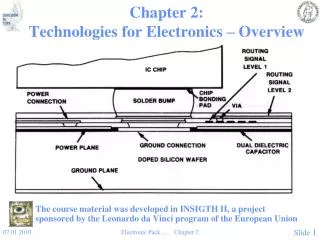
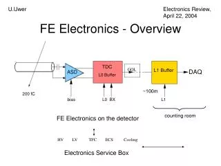
HB Backplane Function • Backplane • ~87 CM LONG • Provides Power • Distributes 40 MHz Clock (3 load max) • Provides path for RBXbus (serial communication bus) • Temperature feedback
Backplane Low Voltage Power Connector • Product Facts • "Inverse-sex" design meets IEC 950 safety requirements • Current rated at 7.8 amperes per contact, 23.5 amperes per module, fully energized • Sequenced right-angle headers available for "make-first/break-last" applications • ACTION PIN press-fit contacts on both headers and receptacle • Contacts designed for up to 250 mating cycles • Recognized to U.S. and Canadian requirements under the Component Recognition Program of Underwriters Laboratories Inc.
Backplane Connectors • Type C and Enhanced Type C Assemblies • Minimum adjacent mounting space required: • 12.7 [.500] • Current Rating: • Per DIN 41612* • Voltage Rating: • 250 VAC • Dielectric Rating: • 1000 VAC • Contact Resistance: • 15 milliohms initial at 100 ma and 50 mv, open circuit
QIE Description • QIE • Charge Integrator Encoder • 4 stage pipelined device (25ns per stage) • charge collection • settling • readout • reset • Inverting and Non-inverting Inputs • Internal non-linear Flash ADC • Outputs • 5 bit mantissa • 2 bit range exponent • 2 bit Cap ID
QIE Specification • QIE Design Specifications • Clock Speed >40MHz • Must accept both polarity of charge input • Positive Input gain relative to Negative Input = 2.67 • Charge sensitivity Lowest Range = 1fC/LSB • In Calibration Mode 1/3 fC/LSB Range 0 only Linear FADC • Maximum Charge = 9670 fC/25ns • Noise 1.5 LSBs in calibration mode, gaussian • Nominal Pedestal • Calibration Mode nominal Ped = 6.5 • Normal Data Mode Ped = .5 • FADC Differential Non-Linearity < .05 LSBs
Channel Control ASIC • The CCA provides the following functions: • The processing and synchronization of data from two QIEs, • The provision of phase-adjusted QIE clocking signals to run the QIE charge integrator and Flash ADC, • Checking of the accuracy of the Capacitor IDs, the Cap IDs from different QIEs should be in synchronization, • The ability to force the QIE to use a given range, • The ability to set Pedestal DAC values, • The ability to issue a test pulse trigger, • The provision of event synchronization checks – a crossing counter will be implemented and checked for accuracy with every beam turn marker, • The ability to send a known pattern to the serial optic link, • The ability to “reset” the QIE at a known and determined time, • And, the ability to send and report on any detected errors at a known and determined time.
QIE/CCA Process Reliability • AMS 0.8u BiCMOS Process (QIE) • Early Failure rate 0.05 - 0.2%; can be reduced to a few ppm by burn-in • Predicted MTTF (25 sqmm, 55 C) is 1.67E8 hours • Expect less than 1 QIE failure per year • HP/Agilent 0.5u CMOS • Well established Commercial Process
Radiation Tolerance • HCAL Radiation Environment • Radiation dose over 10yrs – 1kRad TID and 4E11 n/cm2 • Electronics • QIE and CCA • QIE – AMS 0.8 mm bi-CMOS process • Test bi-polars (TID+bulk damage) and MOS circuits (SEU) • CCA – HP 0.5 mm bulk-CMOS process • Test MOS circuits (SEU) • Serializer – developed in rad hard process • LV regulators – developed in rad hard process • LEDs, other support components – need to test • Studies performed at Indiana U. Cyclotron (200 MeV protons) • Bulk Damage studies • Bi-polars dosed to fluence equivalent of 5E11 n/cm2 • SEU studies • AMS and HP test registers
Pre-irradiation Post-irradiation (6 weeks) 150.0 150.0 b = 95.1 b = 104 15.0 /div Beta 15.0 /div Beta Operating point –10mA Operating point –10mA 0 0 -1E-02 -1E-02 Decade/div Decade/div Current Current Bi-polar Radiation Studies for QIE • Bi-polars from AMS 0.8 mm bi-CMOS process • Beta for npn-transistors dropped by 5-10% after equivalent of 5E11 n/cm2
SEU Studies for QIE and CCA • Test registers (min. feature size, min+guard ring, 2Xmin+guard ring, SEU tolerant) • Xsec results for AMS and HP processes • (1-10)E-15 SEU per n/cm2 per cell (depending on angle) for conservative design using 2Xmin feature size + guard ring • For a complex ASIC with 1000 cells and a fluence of 4E11n/cm2 over a 10 yr operating period • Expect .04-.4 of an upset per ASIC per year
GOL Design Specifications • Synchronous (constant latency) • Transmission speed • fast: 1.6 Gbps , 32 bit data input @ 40 MHz • slow: 0.8 Gbps , 16 bit data input @ 40 MHz • Two encoding schemes • G-Link • Fiber channel (8B/10B) • Interfaces for control and status registers • I2C • JTAG
Gigabit link (G-Link, 8B/10B optional) G-Link (0.8 Gbps) Encoder 1.6 Gbps Data[31:0] 16 20 32 Data Laser Serializer Interface Driver (15) G-Link 8B/10B Clk40 Encoder Laser diode I2C Control & 50 Line Driver Out+ Status PLL JTAG Out- Registers
GOL Radiation hardness • Deep submicron (0.25 um) CMOS • Enclosed CMOS transistors • Triple voting in state machines • Up-sizing of PLL components • Auto-error correction in Config. registers
Rad Tolerant Voltage Regulator • Developed by ST Microelectronics • Specified by CERN RD49 • Shown to be Rad Hard • Presently fixing overvoltage protection • Prepreduction parts due June 2001 • Production parts late 2001
Conclusions • Need to finalize RBX design • Readout Card connector and mechanics cannot be finalized • Backplane production on hold • Our Goal is to have a working FE/DAQ slice by Summer ’01 • We would like to have a production RBX to test clock distribution, noise, …