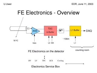
FE Electronics - Overview
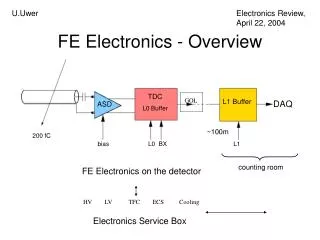
FE Electronics - Overview. TDC L0 Buffer. GOL. L1 Buffer. DAQ. ASD. ~100m. 200 fC. bias. L0 BX. L1. counting room. FE Electronics on the detector. HV. LV. TFC. ECS. Cooling. Electronics Service Box. U.Uwer. Electronics Review, April 22, 2004. 6 m. T3. T2. T1. OT. IT.

FE Electronics - Overview
E N D
Presentation Transcript
FE Electronics - Overview TDC L0 Buffer GOL L1 Buffer DAQ ASD ~100m 200 fC bias L0 BX L1 counting room FE Electronics on the detector HV LV TFC ECS Cooling Electronics Service Box U.Uwer Electronics Review, April 22, 2004
6 m T3 T2 T1 OT IT 5 m TT LHCb Outer Tracker • Straw Tube Drift Chamber • 5mm diameter straw tubes, single straw tube length ~2.5m • ArCO2 / ArCO2CF4 • max. drift times ~44ns • max. occupancy ~ 7% (MC study) • 56k channels • L0 Requirements: • Max. L0 trigger rate is 1.1 MHz • Max. readout time /event is 900 ns • L0 buffer with 160 events (4.0 s) 264 Module
Straw Module 5mm 64 Straws X 2 64 Straws Cathode Grounding tongues
Connector: To HV board Alu coating shield Conductive Kapton Conductive Kapton Gas GLUE (isolating) Alu coating shield ALU Kapton foil for gas tightness Carbon / epoxy skin Module Interface to FE Electronics: Feed-through board defines ground ref.
TFC TFC ECS ECS Power (HV,LV) Power (HV,LV) Fibers to L1 Buffer Fibers to L1 Buffer TFC ECS HV L1 LV GOL LV Reg OTIS OTIS ASDBLR ASDBLR ASDBLR HV boards Fibers to L1 Buffer Fibers to L1 Buffer TFC TFC ECS ECS Power (HV,LV) Power (HV,LV) FE Electronics tot. dose < 10krad FE Box ASDBLR Module End: 128 channels 16 ASDBLR chips 4 OTIS TDC chips 1 optical link: 1.6 Gbit/s Outer Tracker: ST1…3 56000 channels 432 optical links
GOL/Aux Board X 1 • Front-end cards: • have to fit inside the closed shielded FE box: 25 x 30 x 4 cm • excellent ground connection to straw-tubes and module reference ground • power dissipation of cards is about 25 W / box→ water cooling • easy access should be maintained TDC boards X 2 ASD boards X 8 HV boards X 4
R=1 MΩ C=330pF Z=316Ω HV Board: • 32 channels / board • Compact capacitors • Operation in air • casting/embedding of caps Capacitors: JOHANSON 302R29W331KV4E Max. Volt.: 4kV Size: 4.6 x 2 x 1.5 mm3
TDC board: • radiation hard OTIS TDC chip • provides bias voltage for ASD • power rooting for ASDBLR card • test pulses for ASDBLR ASD board: ASDBLR Chip ATLAS DMILL version joined ATLAS chip order 28 wafers à1042 chips
OTIS TDC Chip Components: • 32 maskable channels • DLL, HitRegister, PrePipeline: 6 bit drift time encoding: playback data feed-in (testing) • Pipeline, Derandomizing Buffer: buffer length: 160 evts ↔ 4.0 μs • Control Algorithm: 2 read-out modes: 1, 2, 3 BX/evt • I2C Slow Control Interface: Programming, ASD bias setting • DAC: ASD-Chip bias Status: • OTIS 1.0 in 2002 • Chip Review in June 2003 • OTIS 1.1 received in Feb 2004 • Submission of OTIS 1.2 in May (final chip)
GOL Auxiliary Board • Connected to 4 OTIS boards • Deserialization of OTIS data using CERN GOL serializer chip • Electrical / optical connections to front-end electronics • Optical data link • Low voltage connections • Slow-Control connections • Fast-control (TFC) connection • Voltage (power) regulation Testing optical data transmission, development of readout test system
FE Electronics Box Mounting against water cooled plate
Services and Distribution Boxes Low / High Voltage supplies, L1 Buffer
Summary and Status of FEE Components Currently preparing ¼ station system test foreseen for Oct 2004: Equip 9 modules with electronics: ~2300 channels (18 FE boxes)
Outer Tracker Electronics: Time Schedule 2004 2005 2006 05/04 Submission of OTIS 1.2 06/04 Order pre-series of full electronics for system test 09/04 Delivery of OTIS 1.2 10/04 Pre-series finished, start system test 12/05 Submission of OTIS engineering run 03/05 Start mass production of front-end boards 06/05 OTIS chips from engineering run 01/06 Start electr. assembly