PCB Workshop
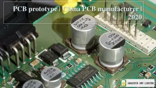
PCB Workshop Michael Hwang m-hwang@northwestern.edu 2/13/2008 Terminology PCB: Printed Circuit Board mil: 1/1000 inch thou: same as mil pitch: Spacing between components (e.g. pins on an IC package) Reflow/wave soldering: industrial methods for mass-production soldering Terminology

PCB Workshop
E N D
Presentation Transcript
PCB Workshop Michael Hwang m-hwang@northwestern.edu 2/13/2008
Terminology • PCB: Printed Circuit Board • mil: 1/1000 inch • thou: same as mil • pitch: Spacing between components (e.g. pins on an IC package) • Reflow/wave soldering: industrial methods for mass-production soldering
Terminology • track/trace: Copper “wires” on the board connecting components. • pad: Exposed copper on which you can solder things. Thru-hole pads often act like vias. • via: A hole in the board that is plated on the inside. Used to connect tracks on different layers of a board. • silkscreen: Print legend on PCB • soldermask: insulating coating that protects covered parts from solder. Mandatory for fine-pitch wave/reflow soldering
Terminology • Thru-hole components: components with leads that go through the circuit board and get soldered on the other side. • Surface-mount (SMD/SMT) components: Components that are meant to be soldered on the same surface on which it is mounted (these are usually smaller and harder to solder).
6-layer PCB cross section Track Pad Insulator (e.g. Fiberglass laminate) Via
Tips: • Use snap grid to keep components at regular intervals • Keep tracks neat • Use large tracks when possible, no smaller than 10 mils. • Keep at least 10 mils between tracks • Put prototyping area in empty space • Add test points
Avoid loops Good: Bad: Loop picks up noise from magnetic fields.
Bypass Capacitors V+ 0.01-0.1 uF
Traxmaker • Abandoned • Graphics bugs • Stability bugs (save and backup often!) • Some moves can’t be undo-ed • Duplicate, place component, etc.
Advanced Circuits Student Discount • http://www.4pcb.com/index.php?load=content&page_id=134 • No minimum order for “33 each” offer, enter “Student” in comments section when ordering. • Single-part orders only, so connect all parts, then saw after they arrive.
Sources: • Jones, David L. PCB Design Tutorial Rev.A. http://alternatezone.com/electronics/pcbdesign.htm