Download
1 / 6
60 likes | 363 Vues
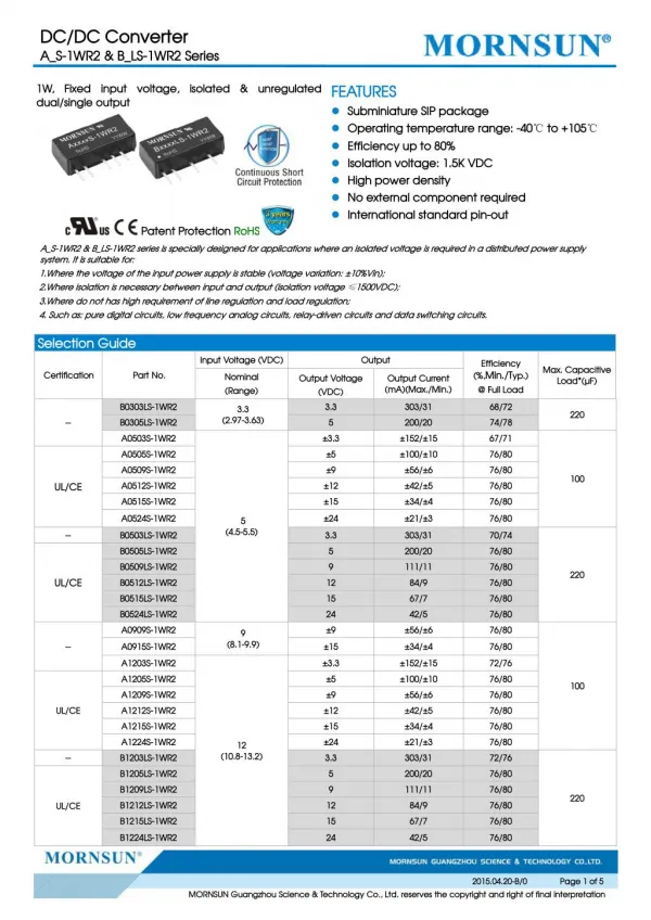
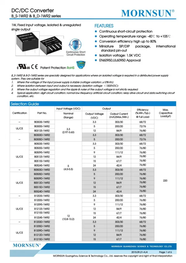
B_S-1WR2 & B-D-1WR2 series are specially designed for applications where an isolated voltage is required in a distributed power supply<br>system. They are suitable for<br>1. Where the voltage of the input power supply is stable (voltage variation: ±10%Vin);<br>2. Where isolation between input and output is necessary (isolation voltage ≤1500VDC);<br>3. Where the output voltage regulation and the ripple & noise of the output voltage is not strictly required;<br>4. Typical application: digit circuit condition; normal low-frequency artificial circuit condition; relay drive circuit and data switching circuit<br>condition, etc.

E N D
DC/DC Converter B_S-1WR2 & B_D-1WR2 series FEATURES Continuous short-circuit protection Operating temperature range: -40℃ to +105℃ Conversion efficiency high up to 80% Miniature SIP/DIP standard pin-out Isolation voltage: 1.5K VDC EN60950,UL60950 Approval 1W, Fixed input voltage, isolated & unregulated single output package, International Patent Protection RoHS B_S-1WR2 & B-D-1WR2 series are specially designed for applications where an isolated voltage is required in a distributed power supply system. They are suitable for 1. Where the voltage of the input power supply is stable (voltage variation: ±10%Vin); 2. Where isolation between input and output is necessary (isolation voltage ≤1500VDC); 3. Where the output voltage regulation and the ripple & noise of the output voltage is not strictly required; 4. Typical application: digit circuit condition; normal low-frequency artificial circuit condition; relay drive circuit and data switching circuit condition, etc. Selection Guide Input Voltage (VDC) Output Efficiency (%,Min./Typ.) @ Full Load Max. Certification Part No. Capacitive Load(µF) Nominal (Range) Output Voltage (VDC) 3.3 5 12 3.3 5 3.3 5 9 12 15 24 3.3 5 9 12 15 24 3.3 5 9 12 15 24 3.3 5 9 12 15 Output Current (mA)(Max./Min.) -- B0303S-1WR2 B0305S-1WR2 B0312S-1WR2 B0303D-1WR2 B0305D-1WR2 B0503S-1WR2 B0505S-1WR2 B0509S-1WR2 B0512S-1WR2 B0515S-1WR2 B0524S-1WR2 B0503D-1WR2 B0505D-1WR2 B0509D-1WR2 B0512D-1WR2 B0515D-1WR2 B0524D-1WR2 B1203S-1WR2 B1205S-1WR2 B1209S-1WR2 B1212S-1WR2 B1215S-1WR2 303/30 200/20 84/9 303/30 200/20 303/30 200/20 111/12 84/9 67/7 42/4 303/30 200/20 111/12 84/9 67/7 42/4 303/30 200/20 111/12 84/9 67/7 42/4 303/30 200/20 111/12 84/9 67/7 68/72 72/76 76/80 68/72 72/76 68/72 76/80 76/80 76/80 76/80 76/80 UL/CE 3.3 (2.97-3.63) -- UL/CE 5 (4.5-5.5) -- 68/72 76/80 76/80 76/80 76/80 76/80 220 UL/CE -- 68/72 76/80 76/80 76/80 76/80 76/80 68/72 76/80 76/80 76/80 76/80 UL/CE 12 B1224S-1WR2 B1203D-1WR2 B1205D-1WR2 B1209D-1WR2 B1212D-1WR2 B1215D-1WR2 (10.8-13.2) -- UL/CE 2015.09.21-A/4 Page 1 of 6 MORNSUN Guangzhou Science & Technology Co., Ltd. reserves the copyright and right of final interpretation
DC/DC Converter B_S-1WR2 & B_D-1WR2 series B1505S-1WR2 B1512S-1WR2 B1515S-1WR2 B1505D-1WR2 B1509D-1WR2 B1515D-1WR2 B2403S-1WR2 B2405S-1WR2 B2409S-1WR2 B2412S-1WR2 B2415S-1WR2 B2424S-1WR2 B2403D-1WR2 B2405D-1WR2 B2409D-1WR2 B2412D-1WR2 B2415D-1WR2 B2424D-1WR2 5 12 15 5 9 15 3.3 5 9 12 15 24 3.3 5 9 12 15 24 200/20 84/9 67/7 200/20 111/12 67/7 303/30 200/20 111/12 84/9 67/7 42/4 303/30 200/20 111/12 84/9 67/7 42/4 76/80 76/80 76/80 76/80 76/80 76/80 68/72 76/80 76/80 76/80 76/80 76/80 15 (13.5-16.5) -- UL/CE 24 (21.6-26.4) -- 68/72 76/80 76/80 76/80 76/80 76/80 UL/CE Input Specifications Item Operating Conditions 3.3V input 5V input 12V input 15V input 24V input Min. -- -- -- -- -- -- -0.7 -0.7 -0.7 -0.7 -0.7 Typ. 404/30 277/20 115/15 83/10 57/17 15 -- -- -- -- -- Filter capacitor Unavailable Max. --/70 --/60 --/50 --/35 --/30 -- 5 9 18 21 30 Unit Input Current (full load / no-load) mA Reflected Ripple Current mA 3.3 input 5V input 12V input 15V input 24V input Surge Voltage (1sec. max.) VDC Input Filter Hot Plug Output Specifications Item Output Voltage Accuracy Operating Conditions Min. Typ. Max. Unit See tolerance envelope graph (Fig. 1) -- -- -- -- -- 18 -- 12 -- 8 -- 7 -- 6 -- 5 -- 60 -- -- -- -- Continuous, self-recovery 3.3VDC output Other output 3.3VDC output 5VDC output 9VDC output 12VDC output 15VDC output 24VDC output ±1.5 ±1.2 -- -- -- -- -- -- 150 ±0.03 1 Input voltage change: ±1% Line Regulation -- Load Regulation 10%-100% load % Ripple & Noise* mVp-p 20MHz bandwidth Full load B24xxS-1WR2/ B24xxD-1WR2/B0524S-1WR2/ B0524D-1WR2 Others Temperature Coefficient %/℃ s Short Circuit Protection** Note: * Ripple and noise are measured by “parallel cable” method, please see DC-DC Converter Application Notes for specific operation; **Supply voltage must be discontinued at the end of short circuit duration for B24xxS-1WR2/ B24xxD-1WR2 series, and B0524S-1WR2/B0524D-1WR2 models. 2015.09.21-A/4 Page 2 of 6 MORNSUN Guangzhou Science & Technology Co., Ltd. reserves the copyright and right of final interpretation
DC/DC Converter B_S-1WR2 & B_D-1WR2 series General Specifications Item Operating Conditions Input-output, with the test time of 1 minute and the leak current lower than 1mA Input-output, isolation voltage 500VDC Input-output, 100KHz/0.1V Derating when operating temperature up to 85℃, (see Fig. 2) Min. Typ. Max. Unit Isolation Voltage 1500 -- -- VDC Isolation Resistance Isolation Capacitance Operating Temperature Storage Temperature Casing Temperature Rise Pin Welding Resistance Temperature Storage Humidity Switching Frequency MTBF 1000 -- -40 -55 -- -- -- -- 3500 -- 20 -- -- 25 -- -- 100 -- -- -- MΩ pF 105 125 -- 300 95 -- -- ℃ Ta=25℃, nominal input, full load output Welding spot is 1.5mm away from the casing, 10 seconds Non-condensing Full load, nominal input voltage MIL-HDFK-217F@25℃ %RH KHz K hours Physical Specifications Casing Material Black flame-retardant heat-proof epoxy resin (UL94-V0) 11.60*6.00*10.16 mm 12.70*10.16*8.20 mm 1.3g(Typ.) 1.8g(Typ.) B_S-1WR2 series B_D-1WR2 series B_S-1WR2 series B_D-1WR2 series Dimensions Weight Cooling Method Free air convection EMC Specifications CE RE ESD CISPR22/EN55022 CISPR22/EN55022 IEC/EN61000-4-2 CLASS B (see Fig. 4 for recommended circuit) CLASS B (see Fig. 4 for recommended circuit) Contact ±8KV perf. Criteria B EMI EMS Product Characteristic Curve 3.3VDC output Tolerance Envelope Curve Other output Tolerance Envelope Curve +10% +15% Output Voltage Accuracy Output Voltage Accuracy Max. +10% +5% Max. +1.0% +5% 0 Typ. Typ. +2.5% 0 -5% Min. -2.5% -7.5% -5% Min. -10% -7.5% -10% -15% -15% 10% 20% 40% 80% 100% 60% 10% 20% Output Current Percentage (Nominal Input Voltage) 40% 80% 100% 60% Output Current Percent (Nominal Input Voltage) Fig. 1 Temperature Derating Curve Output Power Percent(%) 120 100 80 60 Safe Operating Area 40 20 0 -40 0 40 85 105 120 Ambient Temp.( Fig. 2 ) ℃ 2015.09.21-A/4 Page 3 of 6 MORNSUN Guangzhou Science & Technology Co., Ltd. reserves the copyright and right of final interpretation
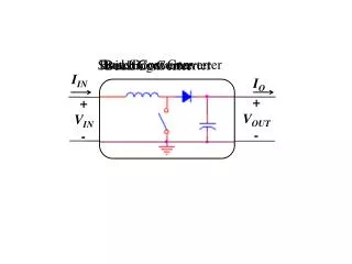
DC/DC Converter B_S-1WR2 & B_D-1WR2 series Design Reference 1. Typical application circuit If it is required to further reduce input and output ripple, a filter capacitor may be connected to the input and output terminals, see Fig.3. Moreover, choosing a suitable filter capacitor is very important, start-up problems may be caused if the capacitance is too large. Under the condition of safe and reliable operation, the recommended capacitive load values are shown in Table 1. Recommended capacitive load value table (Table 1) Vin(VDC) Cin(µF) 3.3/5 4.7 12 2.2 Vo (VDC) 3.3/5 9 Cout(µF) 10 4.7 +Vo Vin DC DC Cout Cin 15 24 -- 2.2 1 -- 12 15 24 2.2 1 0.47 GND 0V Fig.3 2. EMC solution-recommended circuit LDM +Vo Vin Vin Input voltage (VDC) 3.3/5/12/15/24 C1 4.7µF /50V DC/DC LOAD C1 C2 EMI C2 Refer to the Cout in Fig.3 LDM 6.8µH GND GND 0V Fig. 4 3. Output load requirements In order to ensure the converter can work reliably with high efficiency, the minimum load should not less than 10% rated load when it is used. If the needed power is indeed small, please parallel a resistor on t the output side ( The sum of the efficient power and resistor consumption power is not less than 10%). 4. For more information please find DC-DC converter application notes on www.mornsun-power.com 2015.09.21-A/4 Page 4 of 6 MORNSUN Guangzhou Science & Technology Co., Ltd. reserves the copyright and right of final interpretation
DC/DC Converter B_S-1WR2 & B_D-1WR2 series Dimensions and Recommended Layout B_S-1WR2 THIRD ANGLE PROJECTION 0.50 [0.020] 10.16 [0.400] Front View 1 2 3 4 4.10 [0.161] ∅1.00 [∅0.039] Note:Grid 2.54*2.54mm 7.62 [0.300] 0.50 [0.020] 0.90 [0.035] 2.54 [0.100] Pin-Out Function Pin 4 1 2 3 0.30 [0.012] GND Vin 0V 1 2 3 4 6.00 [0.236] Bottom View 11.60 [0.457] +Vo Note: Unit :mm[inch] Pin section tolerances :±0.10[±0.004] General tolerances:±0.25[±0.010] 1100000301-B0 Dimensions and Recommended Layout B_D-1WR2 THIRD ANGLE PROJECTION ∅1.00 [∅0.039] 7.70 [0.303] 8.20 [0.323] 4.10 [0.161] Front view 7 5 4 1 0.50 [0.020] 0.30 [0.012] Note:Grid 2.54*2.54mm 12.70 [0.500] 5.10 [0.201] 7.62 [0.300] 4 1 Pin-Out 10.16 [0.400] 7.62 [0.300] Function GND Vin +Vo Pin Bottom view 1 4 5 7 7 5 ∅1.00 [∅0.039] 5.08 [0.200] 0V Note: Unit :mm[inch] Pin section tolerances:±0.10[±0.004] General tolerances:±0.25[±0.010] 1100000501-B0 2015.09.21-A/4 Page 5 of 6 MORNSUN Guangzhou Science & Technology Co., Ltd. reserves the copyright and right of final interpretation
DC/DC Converter B_S-1WR2 & B_D-1WR2 series Notes: 1. Packing information please refer to Product Packing Information which can be downloaded from www.mornsun-power.com. Packing bag number: 58200003(B_S-1WR2), 58200011(B_D-1WR2); If the product is not operated within the required load range, the product performance cannot be guaranteed to comply with all parameters in the datasheet; The maximum capacitive load offered were tested at nominal input voltage and full load; Unless otherwise specified, parameters in this datasheet were measured under the conditions of Ta=25℃ input voltage and rated output load; All index testing methods in this datasheet are based on our Company’s corporate standards; The performance parameters of the product models listed in this manual are as above, but some parameters of non-standard model products may exceed the requirements mentioned above. Please contact our technicians directly for specific information; We can provide product customization service; Specifications are subject to change without prior notice. 2. 3. 4. ℃, humidity<75% with nominal 5. 6. 7. 8. MORNSUN Guangzhou Science & Technology Co., Ltd. Address: No. 5, Kehui St. 1, Kehui Development Center, Science Ave., Guangzhou Science City, Luogang District, Guangzhou, P. R. China Tel: 86-20-38601850-8801 Fax: 86-20-38601272 E-mail: info@mornsun.cn 2015.09.21-A/4 Page 6 of 6 MORNSUN Guangzhou Science & Technology Co., Ltd. reserves the copyright and right of final interpretation