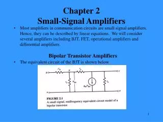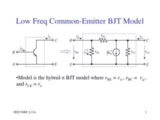
Basic BJT Small-Signal Model
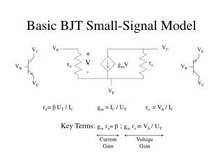
V C. V B. + V -. r o. r p. g m V. V E. Current Gain. Voltage Gain. Basic BJT Small-Signal Model. V C. V E. V B. V B. V E. V C. r p = b U T / I C. g m = I C / U T. r o = V A / I C. Key Terms: g m r p = b ; g m r o = V A / U T. Computing Small-Signal Models.

Basic BJT Small-Signal Model
E N D
Presentation Transcript
VC VB + V - ro rp gmV VE Current Gain Voltage Gain Basic BJT Small-Signal Model VC VE VB VB VE VC rp= bUT / IC gm = IC / UT ro = VA / IC Key Terms: gmrp= b ; gmro = VA /UT
Computing Small-Signal Models Forward-Active Model: (Exponential Form) VCE/VA VBE/UT IC = IC0 e e dIC VCE/UT VBE/UT gm = = IC0 e e (1 / UT) = IC / UT dVBE dIC VCE/VA VBE/UT 1/ ro = = IC0 e e (1 / VA) = IC / VA dVCE
GND GND GND GND GND GND GND GND Basic BJT Small-Signal Model Current Gain Voltage Gain Iout Vdd ro Iref Iin Vin Vout Vout + V - Vin rp Iout gmV + V - rp Iin gmV AV= gmro = VA /UT AI= gmrp= b
Basic Frequency Effects Cje= base-emitter depletion capacitance (forward biased) Cjbc= base-collector depletion capacitance (reversed biased) Cb = Base-Charging Capacitance of the Small Signal BJT Model Modifying Charge from the Base when changing Base voltage: Cb = tF gm Cp= Cje+ Cb; Cm= Cjbc
BJT Small-Signal Model Cm VB VC + V - ro gmV rp Cp VE Basic measures of Frequency Characteristics: fT
Current Gain versus Frequency 2 10 b0 1 10 Collector current / Base current 0 10 fT 3 4 5 6 7 8 9 10 10 10 10 10 10 10 Frequency (Hz)
Additional Effects Series Resistance (rb, rc, re) ---- Finite conductivity of doped regions Collector-Base Resistance of the Small Signal BJT Model (rµ) In general, rµ³ 10 boro for the npn BJT and about 2-5 boro for the lateral pnp BJT