Download
1 / 104
2.26k likes | 4.52k Vues
Section 5.6 Small Signal Model & Analysis. Quiz No 1 DE 27 (CE). 06-03-07. State the purpose and four steps (each) that are to be taken for carrying out DC Analysis (b) Small signal Analysis. The operation of the transistor as an amplifier.

E N D
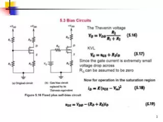
Quiz No 1 DE 27 (CE) 06-03-07 State the purpose and four steps (each) that are to be taken for carrying out • DC Analysis (b) Small signal Analysis
Conceptual circuit with the signal source eliminated . (vbe =0)
DC Analysis Signal source eliminated Active Mode Verification VC>VB-0.4 V
The collector Current & Trans-conductance For vbe<< VT, the transistor behaves as a voltage-controlled current device The trans-conductance of the controlled source is gm Output resistance is infinity
Linear operation of the transistor under the small-signal condition:
Large Signal Model Small Signal Model
Figure 5.51 Two slightly different versions of the simplified hybrid-p model for the small-signal operation of the BJT.
Figure 5.52 Two slightly different versions of what is known as the T model of the BJT.
Small Signal Analysis • Coupling Capacitors • Couples the input signal vito the emitter while blocks the DC signals • Don’t let dc biasing established by VCC&VEE be disturbed. when vi is connected • Capacitor is of very large value –infinite, acts as short circuit at signal frequency of interest.
Application (Steps) : Small Signal Model • Suppress ac independent sources • ac Voltage Sources be short circuited • ac Current Sources be open circuited • Capacitors be Open circuited • Determine DC operating Point IC • Suppress DC independent sources • DC Voltage Sources be short circuited • DC Current Sources be open circuited • Capacitors be short circuited • Replace BJT with small signal Model • Analyze the resulting circuit of find voltage gain & input/output resistance Active Mode Verification VBE > 0.7 V VC> VB-0.4 V Small Signal Analysis
The Early Effect • In real world • (a) Collector current does show some dependence on collector voltage • (b) Characteristics are not perfectly horizontal line
Figure 5.19 (a) Conceptual circuit for measuring the iC –vCE characteristics of the BJT. (b) The iC –vCE characteristics of a practical BJT.
Figure 5.58 The hybrid-pi small-signal model, in its two versions, with the resistance ro included.
The hybrid- small-signal model, with the resistance ro included.
Problem 5.130 • Find the common-emitter amplifier shown in Fig. P5.130, Let VCC =9V, R1 = 27kΩ, R2 = 15kΩ, RE = 1.2kΩ, and Rc = 2.2kΩ. The transistor has β = 100 and VA = 100 V. Calculate the dc bias current IE. If the amplifier operates between a source for which Rsig = 10 kΩ and a load of 2kΩ replace the transistor with its hybrid-Π model, and find the value of Rm, the voltage gain and the current gain
Figure P5.130 DC Analysis Suppress the AC (independent Sources) Short Circuit Voltage Sources Open Circuit the Capacitors Calculate DC Node Voltages & Loop Currents
Figure P5.130 DC Analysis β = 100 , α = 0.99 VA = 100V IE = ?, Rin = ?, overall gain vo/vsig, io/i1
Solution P5.130 • DC Values 1.92 mA 9.64 KΩ 3.21 V 1.94 mA
1.92 mA 9.64 KΩ 3.21 V 1.94 mA Solution P5.130 • Check for Mode ACTIVE MODE VCB > - 0.4 V
Solution P5.130 • Small Signal Model IC = 1.92 mA VT = 25 mV β = 100 , α = 0.99 VA = 100 V
Single Stage BJT Amplifier • Three Configurations • Common Emitter (CE) • Common Emitter (CE) with Emitter Resistance • Common Base (CB) • Common Collector (CC)
Figure 5.60(a) A common-emitter amplifier using the structure of Fig. 5.59.
Amplifiers Configurations Common Emitter
Amplifiers Configurations Common Emitter DC Analysis Suppress Independent ac Source Voltage source ----- Short Cct Current Sources --- Open Capacitors ---- Open Cct Redraw the Circuit Analysis VC VB IE=I IC=αIE IB=(β+1)IE VE VC=VCC-ICRC VB=-IBRB VE=VB-VBE gm=Ic/VT rл=β/gm re=α/gm
Amplifiers Configurations Common Emitter Small Signal Analysis Suppress Independent DC Source Voltage source ----- Short Cct Current Sources --- Open Capacitors ---- Short Cct Redraw the Circuit by replacing BJT With pi Model Analysis gm=Ic/VT rл=β/gm re=α/gm Find Rin, Rout, Voltage Gain vo/vi
Common Emitter + vbe - Short Circuit Current Gain Ais Ais = ios/ii ios=-gmvbe vbe=vi=iiRin Ais=-gmRin Rin=RB||rл Rout=RC|RL
Summary : CE Input Resistance Low to moderate typically a few kilohms Output Resistance Output Resistance is relatively low Open Circuit Voltage Gain Voltage gain of a few hundred Short Circuit Current Gain Current gain equal to β
Figure 5.61 (a) A common-emitter amplifier with an emitter resistance Re.
Redraw the circuit for DC analysis Redraw the circuit for Small Signal pi model analysis Quiz No 2 (DE 27 CE) 13-03-2007
Figure 5.61 (a) A common-emitter amplifier with an emitter resistance Re.
Figure 5.61 (a) A common-emitter amplifier with an emitter resistance Re.
Small Signal Analysis : CE with Emitter ResistanceInput Resistance Multiplication by a factor (1+β) is known as the Resistance Reflection Rule. Analysis
Small Signal Analysis : CE with Emitter ResistanceVoltage Gain Voltage gain is lower than that of CE because of the additional term (1+β)Re
Small Signal Analysis : CE with Emitter ResistanceCurrent Gain