Download
1 / 2
20 likes | 169 Vues
Remote Doping and Charge Transport in Single PbSe NW Field-Effect Transistors Cherie Kagan, University of Pennsylvania, DMR 0805155.

E N D
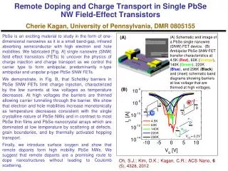
Remote Doping and Charge Transport in Single PbSe NW Field-Effect TransistorsCherie Kagan, University of Pennsylvania, DMR 0805155 PbSe is an exciting material to study in the form of one-dimensional nanowires as it is a small band-gap, infrared absorbing semiconductor with high electron and hole mobilities. We fabricated [Fig. A] single nanowire (SNW) field effect transistors (FETs) to uncover the physics of charge injection and charge transport as we control the carrier type to form ambipolar, predominantly n-type ambipolar and unipolar p-type PbSe SNW FETs. We demonstrate, in Fig. B, that Schottky barriers in PbSe SNW FETs limit charge injection, characterized by the low currents at low voltages as temperature decreases. At high voltages the barriers are thinned allowing carrier tunneling through the barrier. We show that electron and hole mobilities increase monotonically as temperature decreases consistent with the single crystalline nature of PbSe NWs and in contrast to most PbSe thin films and PbSe nanocrystal arrays which are dominated at low temperature by scattering at defects, grain boundaries, and by thermally activated hopping transport. Finally, we introduce surface oxygen and show that remote dopants form high mobility PbSe NWs. We suggest that remote dopants are a promising route to dope nanostructures without leading to Coulomb scattering. (A) (A) Schematic and image of a PbSe single nanowire (SNW) FET device. (B) Ambipolar PbSe SNW-FET transfer characteristics at 4.5K (Red), 60K (Orange), 140K (Green), 220K (Blue), and 298K (Black) and (inset) schematic band diagrams showing barriers at low voltage that are thinned at high voltages. (B) Oh, S.J.; Kim, D.K.; Kagan, C.R.; ACS Nano, 6 (5), 4328, 2012
Sharing the Science of Nanoscale MaterialsCherie Kagan, University of Pennsylvania, DMR 0805155 Nanoday: taking science out to the Philadelphia Community (A) Graduate students from the Kagan group gave demonstrations on the physics of nanoscale materials to families visiting the Northern Lights Community Center for Nanoday, as part of Philly Science Week [Fig. (A, B)]. Two undergraduate students, Tarun Vemulkar [Fig. (B)] and Silvia Chan [Fig. (C)], worked with fellow graduate students to electrically probe charge transport in nanowire transistors. Controlling the nanowire environment impacts its measured transport characteristics. Silvia is now starting her doctorate studies at UC-Santa Barbara and Tarun is starting his PhD at Cambridge University. Undergraduate Research (C) (B)