JFET
The junction-gate field-effect transistor (JFET) is one of the simplest types of field-effect transistor. ... Unlike bipolar junction transistors, JFETs are exclusively voltage-controlled in that they do not need a biasing current. Electric charge flows through a semiconducting channel between source and drain terminals.

JFET
E N D
Presentation Transcript
OUTLINE OUTLINE • Field Effect Transistor (FET) • Junction Field Effect Transistor (JFET) • Construction of JFET • Theory of Operation • I-V Characteristic Curve • Pinch off Voltage (VP) • Saturation Level • Break Down Region • Ohmic Region • Cut off Voltage • Advantages • Disadvantages • Application of JFET
INTRODUCTION The ordinary or bipolar transistor has two main disadvantage. • It has a low input impedance • It has considerable noise level To overcome this problem Field effect transistor (FET) is introduced because of its: • High input impedance • Low noise level than ordinary transistor And Junction Field Effect Transistor (JFET) is a type of FET.
Field Effect Transistor (FET) OUTLINE • FET is a voltage controled device. • It consists of three terminal . • • Gate • • Source • • Drain • It is classified as four types. FET JFET MOSFET MESFET MISFET
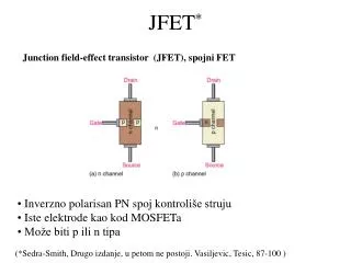
Junction Field Effect Transistor (JFET) OUTLINE • Junction Field Effect Transistor is a three terminal semiconductor device in which • current conducted by one type of carrier i.e. by electron or hole.
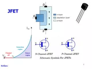
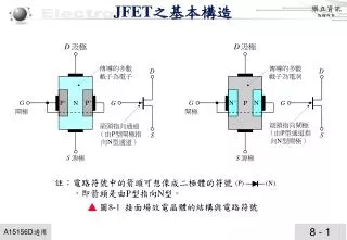
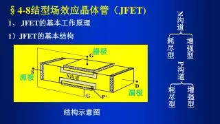
CONSTRUCTION OF (JFET) OUTLINE • Source: The terminal through which the • majority carriers enter into the channel, is • called the source terminal S . • Drain: The terminal, through which the • majority carriers leave from the channel, is • called the drain terminal D . • Gate: There are two internally connected • heavily doped impurity regions to create two • P-N junctions. These impurity regions are • called the gate terminal G. • Channel: The region between the source • and drain, sandwiched between the two gates • is called the channel .
TYPES OF (JFET) OUTLINE • It has two types: • • n- Channel JFET • • p- Channel JFET
SYMBOLS OF (JFET) OUTLINE Drain Drain • • Gate Gate •• • Source • Source n-channel JFETp-channel JFET
FEATURES OF JFET • JFET is a voltage controlled device i.e. input voltage (VGS) control the output current (ID). • Because of reverse bias it has high input impedance. • JFET is a unipolar device,as current conduction is due to only one type charge carriers. • In JFETs, the width of a junction is used to control the effective crosssectional area of the channel through which current conducts. • It is always operated with Gate-Source p-n junction in reverse bias. • In JFET the gate current is zero i.e. IG=0
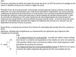
THEORY OF OPERATION • (i) When gate-source voltage(VGS) is applied and drain-source voltage is zero i.e. VDS= 0V • When VGS = 0v , two depletion layers & channel are formed normally. • When VGS increase negatively i.e. 0V > VGS > VGS(off) , depletion layers are also increased and • channel will be decrease. • When VGS=VGS(off), depletion layer will touch each other and channel will totally removed. So no • current can flow through the channel.
THEORY OF OPERATION • (ii) When drain-source voltage (VDS) is applied at constant gate-source voltage (VGS) : • Now reverse bias at the drain end is larger than • source end and so the depletion layer is wider at • the drain end than source end. • When VDS increases i.e. 0v < VDS < VP , depletion layer at • drain end is gradually increased and drain current also • increased. • When VDS = VP the channel is effectively closed at drain • end and it does not allow further increase of drain • current. So the drain current will become constant.
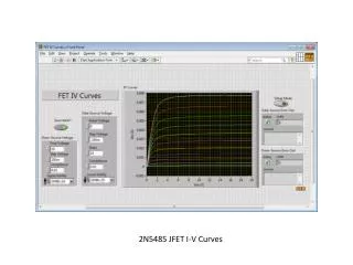
I-V Characteristic Curve • It is the curve between drain current (ID)and drain-source voltage (VDS)for different • gate-source voltage (VGS). It can be characterized as: • For VGS=0v the drain current is maximum. It’s denoted as IDSS and called shorted • gate drain current. • Then if VGS increases Drain current ID decreases (ID < IDSS) even though VDS is • increased. • When VGS reaches a certain value, the drain current will be decreased to zero. • For different VGS, the ID will become constant after pinch off voltage (VP) though • VDS is increased.
Pinch off Voltage (VP) • It is the minimum drain source voltage at which the drain current essentially • become constant.
Saturation Level • After pinch off voltage the drain current become constant, this constant level is • known as saturation level .
Ohmic Region • The region behind the pinch off voltage where the drain current increase rapidly is • known as Ohmic Region.
Break Down Region • It is the region, when the drain-source voltage (VDS) is high enough to cause the • JFET’s resistive channel to breakdown and pass uncontrolled maximum current .
Cut off Voltage • The gate-source voltage, when the drain current become zero is called cutoff voltage. Which is usually denoted as VGS(off).
P-Channel JFET • p-channel is forming between two layers n-type materials. • Four ohmic terminals. • 2 p-n junctions. • 2 depletion regions. • By increase the width of depletion region the p-channel is reduced by apply voltage S and P. • This is cotrolled by S and G voltage.
Advantages • It is simpler to fabricate, smaller in size. • It has longer life and higher efficiency. • It has high input impedance. • It has negative temperature coefficient of resistance . • It has high power gain.
Disdvantages • Greater susceptibility to damage in its handling. • JFET has low voltage gain.
Applications of JFET • Voltage controlled resistor. • Analog switch or gate. • Act as an amplifier. • Low-noise amplifier. • Constant current source.