Industrial PC Control Panel for Enhanced Performance
Install special connectors and expand cables with a panel featuring dual cooling fans for positive airflow, adjustable shock-resistant clamps, 14-slot PC bus board, 300W industrial switch power supply, and reinforced metal chassis with removable air filters. Additional features include power on/off button, status indicators, reset key, keyboard-lock function, dust-proof lockable door, and various internal registers for CPU operations. Memory organization and device functionalities are also explained in detail.

Industrial PC Control Panel for Enhanced Performance
E N D
Presentation Transcript
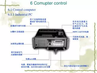
6 Comupter control 用于安装特殊连接器或扩展电缆的面板 双冷却风扇建立空气正压力,经过滤的空气在机箱内流通 防震的可调节夹钳 14槽PC总线底版 300W工业开关电源 可拆卸式光驱、软驱框架 加固型金属机箱 带可拆卸空气 过滤器的面板 电源on/off键 电源、硬盘及键盘的状态指示灯 RESET键、KEYBOARD-LOCK键 防尘与保证运行安全的带锁门 6.1 Control computer 6.1.1 Industrial PC
Accumulator Register • accumulator register - where data for the input to ALU is temporarily stored • First, the CPU needs to be supplied with the address of the required memory location where an instruction, or data, is stored so that it can access it via address bus • When this is done, the instruction, or data, is read into the CPU via data bus • Since only one memory location can be accessed at any one time, temporary storage has to be used when, for example, numbers have to be manipulated (added, subtracted etc.) • So, if 2 numbers are to be added, one number is fetched from its memory location and placed into an accumulator register while the CPU fetches the other number from another memory location • Once they are added to each other, the result is placed to the accumulator register for temporary storage
Flag register • The flag register (or, status register, or condition code register) - contains the result of the latest process carried out by ALU • it contains individual bits, each having special significance. The bits are called flags. • The status of the latest operation is indicated by a flag • each flag may be set (e.I.1) or reset (e.I. 0) depending on the status
Program counter register • It keeps track of the CPUs position in the program • it contains the address of the memory location of the next program instruction, hence the alternative name instruction pointer • as each instruction is executed, the program counter register is updated • the program counter is incremented each time so that the CPU executes instructions sequentially, unless some special commands (e.g. JUMP) are given to change it out of the sequence • not accessible by the programmer
Some other registers • memory address register (MAR)contains the address of the data (like an 'address book' of all the addressed where various data are stored) • instruction register (IR) stores an instruction. After fetching an instruction from the memory, the CPU stores it in the IR. It can then be decoded and used to execute an operation • general purpose register - temporary storage for data or addresses; also for transfers between various other registers • stack pointer register (SP) - holds the address of the top of the stack in RAM. Stack - special area of RAM where program counter values can be stored when a subroutine of a program is being executed
Memory organisation • The memory unit stores binary data • The size of the memory is determined by the number of wires in the address bus • For data permanently stored - a read-only memory (ROM) device is used • If the content of ROM can be altered (somehow) it is referred to as erasable programmable ROM (EPROM) • Temporary data - I.e. the data currently being operated on - is stored in read/write memory called random-access memory (RAM) • When switched ON, the program from keyboard or other input device is loaded in RAM
Memory devices • typical EPROM: a series of small electronic circuits - cells - which can store charge. The program is stored by producing a pattern of charged/uncharged cells • The pattern is erasable using UV light (through a quartz window on the top of the device) • EEPROM is electronically erasable, which is easier - but, the chip itself is more expensive • Static RAM (SRAM) - based on bistable circuit. The output remains in its state until a subsequent valid input is issued. The bit cell of a SRAM is relatively large so it cannot be densely packed within a given area of silicon, which is a disadvantage
Memory devices • The Dynamic RAM (DRAM) bit cell is a capacitor capable of storing charge. A single data line is used both to write data into the bit cell and to read data from it. The charge tends to leak out of the capacitor causing its voltage to drop, so DRAM needs to be periodically refreshed. This is why it is called 'dynamic' RAM. • Refreshing is done by reading data and writing it back to the same cell. • usually, circuitry external to the memory chip is used for refreshing • Packing density is higher for DRAMs than SRAMs, so more memory can be implemented in the given area. • Modern DRAM have their refresh control logic on-chip
Memory requirements • there is a considerable difference in memory requirements between embedded and computing applications • in both classes the 'system memory' term is used to refer to the part which is directly accessible to the microprocessor, as opposed to the storage media such as a magnetic disc or tape drive etc. • in embedded systems, the memory consists of varying amounts of non-volatile memory (ROM), the contents of which will not be lost in the case of power loss, and volatile memory (RAM) which loses its content if power supply is removed. • Once information (program and constant data) is written into non-volatile memory it can be considered permanent and it is referred to as firmware
Memory requirements • the programs in embedded systems are typically small. • For example, a washing machine control program may require only 2k bytes of memory. • For more demanding applications, such as communication controllers, several hundreds of kilobytes of ROM may be required
Input/Output devices • Input and output devices provide the means by which a microprocessor system can convey information between itself and the outside world. • Microprocesor has to accept input information, respond to it and produce output signals to implement required control • There may be inputs from sensors to provide data to the microprocessor and outputs such as relays or motors • The term peripheral is used for a device connected to a microprocessor. Such devices add specific functions, like timers and interrupt controllers to the mP system
Input/Output devices • But, they cannot be, in general, directly connected to a microprocessor due to a lack of compatibility with the bus system in signal forms and levels • A circuit, called an interface, is used between the peripheral devices and the microprocessor to overcome this problem - to perform the required conversion • n general, I/O devices contain 2 types of registers: • control, or status register - through which the program can control the mode of operation of the I/O device • the second type of register provides the data path to enable the microprocessor system to read/write information to the outside world
Buses • Data bus. To transfer the data associated with the processing function of the microprocessor. Word lengths may be 4,8,16 or 32 bits. Each wire in the bus carries a binary signal (0 or 1). The more wires the data bus has the longer the word length that can be used. Thus, for the word length of 4 bits, the number of values that can be transferred is 24=16
Buses • Address bus which contains the address of a specific memory location for accessing stored data.It carries signals which indicate where data is to be found so that certain memory locations can be selected. When a particular address is selected by its address being placed on the address bus, only that location is open for communication with CPU. The CPU communicates with only one address at a time. Usually address bus contains 16 wires • Control bus. This carries the control signals to the memory and the I/O devices. It is used to synchronise separate elements. The system clock signal is carried by the control bus, for example.
Number representation - a brief reminder • binary and hexadecimal number representations are commonly used in programming • to convert a binary number into a hexadecimal number it is handy to group digits in fours, because 24=16 and each block (of 4) can be represented by a single hexadecimal character • For example: a binary number 1011100100011110 grouped in fours gives: 1011 1001 0001 1110 B 9 1 E
Conversion table Hexadecimal Decimal Binary 0 0 0 1 1 1 2 2 10 3 3 11 4 4 100 5 5 101 6 6 110 7 7 111 8 8 1000 9 9 1001 A 10 1010 B 11 1011 C 12 1100 D 13 1101 E 14 1110 F 15 1111
Memory mapping • The memory map designed to meet requirements of the application • It will be used by a hardware designer to partition the address space so that the address range of the memory devices in the system corresponds to the address range specified by the memory map • This is achieved by means of a address decoder • An example is shown in the following figures
Chip Select signal • when the correct address appears on the address bus the output from the decoding circuit changes to the logic state necessary to activate the device to supply/receive the data • the signal is called ‘Chip Select’ signal (CS/); often set as active low • a decoder is a combinational logic circuit which will decode a binary code and activate output signals according to the states of the lines applied at the input
Address decoding • let’s have a look at a typical 8-bit data bus whose wires (8) are numbered: D0 - first wire: least significant bit (LSB) D7 - eighth wire: most signif. bit wire (MSB) • and the 16-bit address bus (see Figure) • in the control bus there’ll be a line dedicated to READ/WRITE: • notation RD/ or WR/ (slash means active low) • a logic circuit decodes the address bus signal and selects the appropriate device
Address decoder: logic gates • the least significant bit is at A12; it remains in a logic state '1' • A12 is passed through an inverter, so that the chip select signal at the output of the decoder is '0' only when A12 is '1' • note that in this case, the chip select signal is set to be 'active low', I.e. CS/ • similar decoding logic for each chip occupying the same amount of memory • if more complicated memory mapping is required, decoder functions are implemented using programmable logic array
Read cycle • It lasts 2 cycles of the clock signal: 1. address of required memory location put on address bus (by CPU), at rising edge 2. while device held at ‘tristate’ level - control bus issues ‘read signal’ (active low) to the device (2nd cycle begins) 3. after delay - valid data placed on data bus 4. levels on the data bus sampled by CPU at falling edge of the 2nd cycle
Write cycle 1.CPU places address at rising edge 2. decoding logic selects correct device 3. 2nd cycle - rising edge: CPU outputs data onto data bus & sets WRITE control bus signal active (LOW) • Note: • memory devices & other I/O components have static logic - so do not depend on clock signal; they read data from data bus when write signal high (inactive) - data must be valid for transition
Choosing a microprocessor systems • the microprocessor system will be originally conceived from a functional requirement. For example, to control a robot arm, or to monitor some process etc. • based on the requirements the system specification will be made Input/Output requirements • the number and type of input/output devices will be based on the number of sensors and actuators needed for the function • communications with other systems in order to provide remote control will be chosen to be compatible with these systems in terms of both hardware and protocols used
Choosing an mP system • complexity of the function to be performed will influence the choice of the processor, the CPU in particular • performance is the most critical factor to be considered and most difficult to assess • number of operations per second IS NOT a sufficiently good indicator of the performance • benchmarking is better - running a representative piece of code to determine the speed of execution • simulator is another good way of assessing the performance
Development environment • the set of tools with which the designer can verify the hardware design , write and test the software and test the complete system are presented in the figure below
Development environment • the prototype hardware is referred to as target system • the software for the target system is written on a computer referred to as the host as it hosts the development tools during the development (nowadays, it is usually a PC) • when the program functions correctly it may be programmed into a ROM device and be permanently installed on a target system • the interface between the host and the target system is a hardware emulator for the target microprocessor. It has the ability to control the execution of the application program • typically, the emulator is a standalone unit
Development environment • alternatively, emulator can be an add-in card to the personal computer (the host) • communication link is usually a simple serial RS232 interface • through that link the host downloads the machine code application program to the emulator and controls and monitors its execution • to the target system emulator appears as would be the real microprocessor
Development cycle • there is a well defined development cycle typical of any product development • The basic cycle is shown schematically in the following diagram: First design Implement design Test design against the spec. Does it meet specifications? Review design Manufacture a product No Yes
Development cycle • the designer enters the application program into the host system using an editor (similar to a word processor). The programming language can be either a high-level (e.g. C) or a low-level (assembler) language • the next step is to convert the source code into the machine code instructions understood by a specific microprocessor. This is done by a language compiler or by an assembler, depending on which language has been used • the output of a compiler will be a file containing the machine code, which when executed by the target microprocessor will perform the functions defined by the source code. This machine code is called object code
Common practice • large programs are often developed as a collection of smaller and more manageable programs. • if a frequent use is made of a particular routine the routine can be placed into a library of commonly used routines for use in any subsequent program. A library consists of the relocatable object code of such routines • nowadays, high-level languages are often used. The benefits include: • improved productivity • less prone to errors • allows more complex data manipulation • program more portable • source program more easily readable • disadvantages: • it generates more object code than an equivalent assembly lang. prog. • compiled object code runs more slowly
Programming Languages • microprocessors perform certain actions as a result of the so called instructions given to the mP. • the collection of these instructions constitute s an instruction set • the form the instructions take is dependent on the type of mP (the manufacturer) • a series of instructions necessary to complete certain task is known as a program. • microprocessors 'understand' only a binary code, which is referred to as a machine code.
Programming Languages • writing a program in binary code is very 'unfriendly' and instructions are not easily identifiable • alternatively, a form of comprehensible shorthand code for the patterns of 'zeros' and 'ones' can be used. Such codes are referred to as mnemonic codes • the term assembly language is used for such a code • it is easier to use than binary code • but, they still have to be translated into the machine code • the conversion can be done by hand using data sheets from the manufacturer, which give binary code for each mnemonic
Programming Languages • there are, however, computer programs that do the conversion - the so called assembler programs • even more easily comprehended are so called high-level programming languages, such as C, BASIC, FORTRAN etc. • they also have to be converted into a machine code by specific computer programs so that mP may be able to use. • high-level languages require more memory to store them when they have been converted to a machine code. Consequently, they take longer to run than the programs written in assembly language
Instruction sets • the set of instructions given to the mP to execute a task is called an instruction set • Generally, instructions can be classified into the following categories: • Data transfer • Arithmetic • Logical • Program control • We shall address briefly each category in turn. They differ depending on the manufacturer, but some are reasonably common to most mP's.
Data transfer • 1. Load • It reads the content of a specified memory location and copies it to the specified register location in the CPU • 2. Store • copies the current contents of a specified register into a specified memory location.
Arithmetic • 3. Add • Adds the contents of a specified memory location to the data in some register • 4. Decrement • subtracts 1 from the content of a specified location. • 5. Compare • indicates whether the contents of a register are greater than, less than or same as the contents of a specified memory location. The result appears as a flag in the status register.
Logical • 6. AND • carries out the logical AND operation with the contents of a specified memory location and the data in some register • 7. EXCLUSIVE OR - (similar to 6, but for exclusive OR) • 8. Logical shift • moving the pattern of bits in the register one place to he left or right by moving zero (0) to the end of the number • 9. Arithmetic shift • moving the pattern of bits one place left/right but with copying of the end number into the vacancy created by shift • 10. Rotate • moving the pattern of bits one place left/right but the bit that spills out is written back into the other end
Program control • 11. Jump • changes the sequence in which the program is executed. So the program counter jumps to some specified location (other than sequential) • 12. Branch • a conditional instruction which might be 'branch if zero' or 'branch if plus'. It is followed if the right conditions are met. • 13. Halt • stops all further microprocessor activities
Example of a flow chart with a branch Decrement the accumulator is accumulator zero?? No Yes Start new program segment Copy accumulator to register X
Flow chart shapes • common meaning of certain shapes used in flow charts: subroutine Start/End Input/Output Decision Process program flow connector
Features & Use of microcontrollers • Advanced high level code generating tools for efficient code generation. • Developers can now automatically build device drivers, boot and glue code that meet their precise specifications through an easy-to-use point and click interface. • Control of complex mechanical system such as multi-axis robotics. The intelligent timer system is capable of monitoring multiple sensors and driving multiple actuators with minimum CPU servicing. • Industrial networking using the industry standards. • Control requiring simultaneous analog signal sampling, such as electric motor control. • Analogue to digital converter systems are capable of timed and synchronous sampling of analogue inputs.
Features & Use of microcontrollers • Modern microprocessors, feature extensive on-chip peripherals like: • Universal Serial Bus (USB) • Host controller • USB Function and • colour LCD controller
State of the art technology • The high-performance CPU core combines: • 32-bit RISC CPU and 16-bit integer DSP unit into a powerful, multitasking core • four-bus structure, • 16-kilobyte (KB) cache and 16-KB X/Y random access memory (RAM). • Processing performance is 208 million instructions per second (MIPS) at 160-MHz operating frequency. • Memory management unit (MMU) • other peripheral functions required for system configuration such as: • a timer, a real time clock, an interrupt controller, and a serial communication interface.
Instruction Set Complexity: CISC vs. RISC • The primary objective of processor designers is to improve performance. Performance is defined as the amount of work that the processor can do in a given period of time. Different instructions perform different amounts of work. • To increase performance, you can either have the processor execute instructions in less time, or make each instruction it executes do more work. Increasing performance by executing instructions in less time means increasing the clock speed of the processor. Making it do more work with each instruction means increasing the power and complexity of each instruction. Ideally you'd like to do both, of course, but it is a design tradeoff; it is hard to make more complex instructions run faster.
1). Comparison element 2). Control element 3). Correction element (actuator) 4). Process element 5). Measurement element