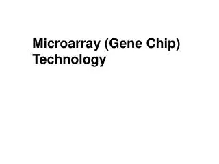
Electroplating Solder Bumping Flip Chip Technology 电镀焊球凸点倒装焊技术
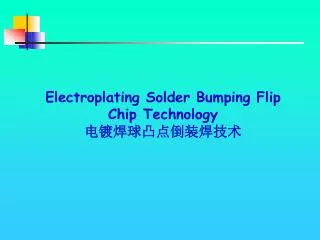
Electroplating Solder Bumping Flip Chip Technology 电镀焊球凸点倒装焊技术. Passivation. Al contact pad. Chip. Electroplated solder bump. Mushrooming. 1. Wafer with Al pad 钝化和金属化晶片. 2. Sputter Under Bump Metal 金属层溅射. 3. Coat with PR 覆盖光胶. 4. Pattern for bump 凸点光刻. solder ball after reflow.

Electroplating Solder Bumping Flip Chip Technology 电镀焊球凸点倒装焊技术
E N D
Presentation Transcript
Electroplating Solder Bumping Flip Chip Technology电镀焊球凸点倒装焊技术
Passivation Al contact pad Chip Electroplated solder bump Mushrooming 1. Wafer with Al pad 钝化和金属化晶片 2. Sputter Under Bump Metal金属层溅射 3. Coat with PR 覆盖光胶 4. Pattern for bump 凸点光刻 solder ball after reflow Chip Chip 5. Electroplating Cu and Sn/Pb焊料电镀 6. Remove Resist 去除光胶 7. Strip Under Bump Metal 去除UBM 8. Reflow回流 Chip UBM Chip Thick photoresist film Chip Chip PR opening Chip Electroplating Solder Bumping Process电镀焊球凸点工艺 Process Flow of Electroplating Solder Bump 电镀焊球凸点工艺流程
Electroplating Solder Bumping Process电镀凸点制备工艺 Peripheral array solder bumps 周边分布凸点 Area array solder bumps 面分布凸点 • The peak temperature of reflow process回流焊峰值温度: 220 ºC. • The effective bump pitch for peripheral array周边分布有效凸点间距: 125 m.
Process Specification工艺参数 • Photoresist Thickness 光刻胶厚度: 40~100 m • Bump Material凸点材料: 63Sn/37Pb • Bump height 凸点高度: 75~140 m • UBM layer凸点下金属层: Ti/W-Cu, Cr-Cu • Min. effective pitch of bump 最小有效凸点间距 : 125 m • I/O array输入/输出分布: peripheral array周边分布 and area array面分布
Flip Chip on Low-Cost Substrate Samples Samples with Different Dimensions PCB上不同尺寸倒装焊样品 Flip Chip on Flexible substrate在软质底板上倒装焊 • Direct chip attach on low-cost PCB, flexible substrate • 已完成在低成本PCB和软质底板上倒装焊工艺的研究 • MCM-L technology 多芯片组装技术.
Stencil Printing Bumping Flip Chip Technology丝网印刷凸点倒装焊技术
Solder Bump Electroless Ni/Au Passivation Chip Electroless UBM and Stencil Printing化学镀UBM和丝网印刷工艺 • The most potential low cost flip chip bumping method. 最具前景的低成本倒装焊凸点制备方法 • Using electroless Ni/Au as UBM system 用化学镀镍/金作为凸点下金属层 • maskless process 无掩膜工艺 • Compatible with SMT process 与表面贴装工艺兼容 • Flexible for different solder alloys适用于不同焊料合金
Wafer preparation晶片制备 (Passivation and Al pads) Zincation Pretreatment锌化预处理 Electroless Ni/Immersion Au化学镀镍/金 Stencil Printing丝网印刷 Solder Reflow and Cleaning焊料回流和清洗 Stencil Printing Process Flow丝网印刷工艺流程 Process flow of Stencil Printing Process丝网印刷工艺流程 (not to scale)
Stencil Printing Process Flow 丝网印刷工艺流程 • Sketch of process flow Electroless Ni/Au Stud (Cross section)化学镀镍/金 Reflow回流 Solder Paste Printing浆料印刷
Process Specification 工艺参数 • I/O pads with a pitch of 400m are used for testing dice The limitation of this process is the pitch of 150 m. 测试芯片I/O凸点间距:400微米 • Thickness of Ni/Au UBM is 5~6m. Ni/Au UBM厚度:5~6微米 • Different solder alloys are available. Solder alloys from different vender: Kester, Multicore, Alpha Metal, Indium,… Different composition: eutectic Pb-Sn, lead free 可应用不同供应商凸点焊料
Samples by Stencil Printing Bumping丝网印刷凸点工艺样品 Flip Chip on PCB for Testing 在PCB上倒装焊测试样品
Reliability Test Design可靠性测试设计 • JEDEC Standard for Test Design JEDEC标准测试设计(Joint Electron Device Engineering Council) Test Dice 测试芯片 Low cost substrate低成本底板 Bumping凸点制备 Mechanical Properties Test (Bump shear)机械测试 Assembly (Bonding and Underfilling)装配工艺 Reliability Test (Thermal Cycling)可靠性测试
Standard Condition Results Electroplating Flip Chip Stencil Printing Flip Chip Multiple Reflows Normal Reflow Profile No degradation after 10 reflows High temperature Storage JESD22-A103-A 150C, Air No degradation after 1000 hours No degradation after 1000 hours Temperature & Humidity 120C and 85%RH No degradation after 100 hours Thermal Cycling JESD22-A104-B -40C~+125C 1cycle/hr Pass 1000 cycles No failure after 1500 cycles Reliability Test Results可靠性测试结果 Both Bumping Process Produce Reliable samples 两种凸点工艺样品的可靠性
Wafer Level Input/Output Redistribution晶片级输入/输出再分布
Wafer Level Input/Output Redistribution Applications 晶片级I/O再分布技术的应用 • Convert chips designed for perimeter wirebond to area flip chip bonding. 可转换已设计芯片,由周边丝键合至面分布倒装焊键合 • Increase I/O density while increase I/O pitch. 增加I/O密度同时增加I/O间距 • Improve reliability and manufacturing yield. 改善可靠性和制造率 • Adapt existing chips designed for wirebonding to flip chip. 在现有已设计的丝键合芯片上应用倒装焊技术
Area Array Peripheral Advantages 优点 WL-Input/Output redistribution will eliminate the underfilling process in Flip Chip Technology! 再分布技术可消除倒装焊技术中填充塑封工艺! Redistribute tight pitch perimeter I/O to loose pitch array bonding and increase package reliability 增加焊点间距和封装可靠性
BCB1 Solder ball BCB2 BCB_1 5m 300m Metal_2 (Ti-W/Cu) 0.5m /5m 120m 250m 100m UBM BCB_2 5m Metal 2 UBM (Ni) 5m Silicon substrate Al pad 80m Passivation 120m Solder ball size (diameter) 300m Solder ball pitch 500m Structure of I/O Redistribution再分布结构 Key Feature : Critical Dimension :
Metal1 Al Sputtering Photolithography Wet etch Passivation PE-CVD SiO2 Photolithography Plasma dry etch BCB 1 Spin coating Photolithography Hard Cure Wafer start BCB 2 Spin coating Photolithography Hard Cure or Metal 2 Al sputtering Photolithography Wet etch Metal 2 Ti-W/Cu seed sputtering Photolithography Copper electroplating Ti-W/Cu seed remove Stencil solder printing or Solder Electroplating Process Flow of Redistribution Test Chip再分布测试芯片工艺流程
Some of Flip Chip Equipment倒装焊设备 Electroplating Station电镀台 Wafer Stencil Printer晶片丝网印刷机 Flip Chip Bonder倒装焊机
Possible Business Relationship 合作方式 • License of the technology 技术许可证 • Joint venture with HKUST injecting the technology 合资:香港科大注入技术 • Contract research - pre-defined deliverable for an agreed amount of $. 合作研究 • Other schemes 开展其它合作模式 • For more information contact 联系人 Prof. Philip Chan陈正豪教授 (852) 2358-7041 Email: eepchan@ust.hk