Download
1 / 14
150 likes | 190 Vues
Discover the overlapping energy bands in semiconductors, including electron configurations, Fermi energy, electrical conductivity, and more. Explore the properties of Group IV, III-V, and II-VI semiconductors, alongside the correlation between lattice parameters and gap sizes.

E N D
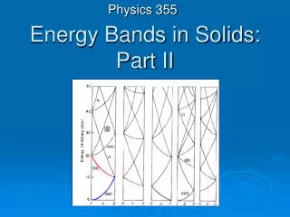
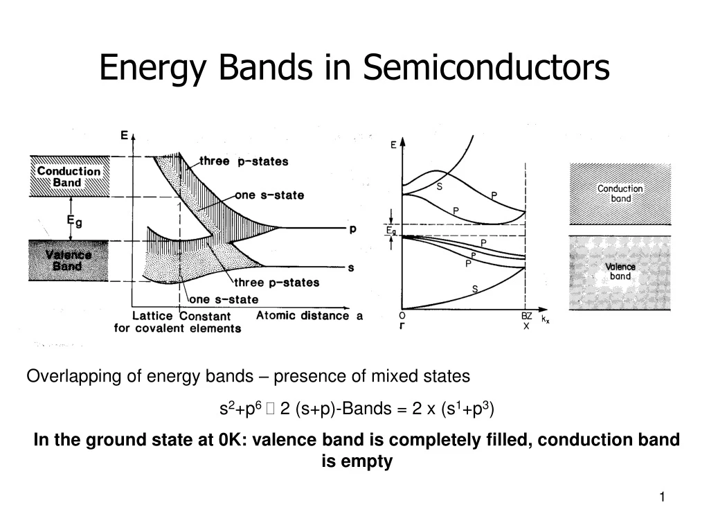
Energy Bands in Semiconductors Overlapping of energy bands – presence of mixed states s2+p6 2 (s+p)-Bands = 2 x (s1+p3) In the ground state at 0K: valence band is completely filled, conduction band is empty
Electron configurations in semiconductors: 4 electrons at the highest atomic energy level Group IV (C, Si, Ge): 2 s2 + 2 p2 Group III-V (GaAs, GaP, AlN, GaN): 2 s2 + p1 + p3 Group II-VI (ZnO, CdS, CdTe): 2 s2+ p4
Pure (intrinsic) semiconductors Electrons with (): Population density: Density of state: Fermi function: Number of electrons in the conduction band: (e-in the CB)
Fermi Energy in Semiconductors Fermi energy: Temperature T = 0K T > 0K Energy The Fermi energy (Fermi level) of semiconductors at 0K is located in the middle of the energy gap
Electrons in the Conduction Band Fermi function:
Electrons in the Conduction Band Number of electrons in the conduction band: Fermi energy: Effective mass: Number of electrons in the conduction band (per unit of volume):
Mobility of electrons and holes Electrical conductivity Density of the charge carriers
Electrical Properties of some Semiconductors Effective mass
Table 14.6. gap energy, mobility of electrons and holes and the effective mass of conduction electrons Lattice parameter(Å) Diamond 3.5670 4.3585 5.4300 5.6568 5.6533 6.0954 6.056 6.4867
Energy Transition of Electrons between Valence Band and Conduction Band* Thermal excitation Photon Electron Optical transition Phonon Cutoff frequency of absorption: * Quantum jump