TDC and PLL work
TDC and PLL work. Jeffrey Prinzie. Previous work. Thesis Low jitter clock generator PhD Radiation tolerant TDC. Low jitter clock generator Concept. Equivalent-time sampling clock Tref + Ts UWB imaging (Tx / Rx) Requires accurate clock Low jitter 51.2 GSa/s eq. time.

TDC and PLL work
E N D
Presentation Transcript
TDC and PLL work Jeffrey Prinzie
Previous work • Thesis • Low jitter clock generator • PhD • Radiation tolerant TDC
Low jitter clock generatorConcept • Equivalent-time sampling clock • Tref + Ts • UWB imaging (Tx / Rx) • Requires accurate clock • Low jitter • 51.2 GSa/s eq. time
Low jitter clock generatorPLL • 3rd order PLL • 2.8 ps RMS jitter • 8 phase generation • Maneatis load VCO • Charge pump PFD • No multiplier • 90nm UMC CMOS
Low jitter clock generatorDTC • 0-1.25ns Delay control • 6 bit • PVT insensitive • 2nd Phase lock
Low jitter clock generatorResults 3.2 ps jitter (system) 4 mW power consumption 19,5 ps
Previous work • Thesis • Low jitter clock generator • PhD • Radiation tolerant TDC
TDCchip 1 • DLL based TDC • DLL → gain/resolution • Td = Tref/N • DLL corrects TID radiation • DLL reduces mismatch effects
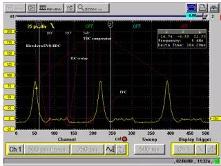
TDCchip 1 • Delay line • Resistive interpolation • 5.8ps resolution • Tref/5N • Mismatch • 156 fs/√ps • Coding • Thermometer code → Binary • Bubble correction • Priority detection • ROM
TDCchip 1 • DLL control loop • Radiation • TID → offset in PD • SEE → lock loss • Combination PFD and Bangbang PD • Speed/Recovery→ PFD • Low offset (calibration) → Bangbang PD
PFD • Deadzone (20ps) • High bandwidth • SEE recovery • Large SPO • Bangbang PD • Low bandwidth (fine adjustment) • Low SPO (1.2 ps 3σ) (TID) • Trade-off: speed vs. ripple (spur)
ProgressChopped phase detector • Bang-Bang-PD: Chopping • Minimizes SPO through radiation • Time domain • Principe • Inject calibration-clock in both inputs • Measure phase difference (offset) • Correct PD • Effective DLL measurement Calibration
Progress: chip 1 • Inject calibration-clock in both inputs • Measure phase difference (offset) • Correct PD • Effective DLL measurement
Progress: chip 1 • Inject calibration-clock in both inputs • Measure phase difference (offset) • Correct PD • Effective DLL measurement
Progress: chip 1 • Inject calibration-clock in both inputs • Measure phase difference (offset) • Correct PD • Effective DLL measurement
Progress: chip 1 • Inject calibration-clock in both inputs • Measure phase difference (offset) • Correct PD • Effective DLL measurement
Progress: chip 1 • Mismatch between 2 Mux • → SPO ( 1.2ps 3σ including measurement) • Reduction of 1/f noise in PD • Increases with radiation • Future improvements • Interleaved BB-PD • Individual calibration of DLL elements
1.75mm 130 µm 0.95mm 370 µm 45 nm TSMC CMOS RF 10 layer
Conclusion • 2 year work on • Time based systems / control loops • PLL, TDC, DTC … • nm CMOS implementation • Jitter / Phase noise optimization • 1 year work on • Radiation effects • Research group • Multiple PhD on radiation tolerant ICs • Amplifier , ΣΔ TDC …