Download

1 / 51
510 likes | 521 Vues
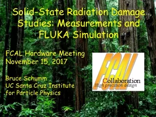
Solid-State Radiation Damage Studies FCAL Workshop Sept 4-5, 2017 Bruce Schumm UC Santa Cruz Institute for Particle Physics. 2 X 0 pre-radiator; introduces a little divergence in shower. Sensor sample. Not shown: 4 X 0 “post radiator” and 8 X 0 “backstop”. Silicon Diode Sensors.

E N D
Solid-State Radiation Damage Studies FCAL Workshop Sept 4-5, 2017 Bruce Schumm UC Santa Cruz Institute for Particle Physics
2 X0 pre-radiator; introduces a little divergence in shower Sensor sample Not shown: 4 X0 “post radiator” and 8 X0 “backstop”
Silicon Diode Sensors • n-bulk (N) and p-bulk (P) • Both float-zone (F) and Magnetic Czochralski (M) for each of N,P • 300-400 m thick bulk • Various manufacturers • Heaviest doses for pad (not strip) sensors 3
NF Type Charge Collection for 300 Mrad @600 V, ~40% charge collection loss (58C annealing) 1-hour annealing steps 300 Mrad Exposure NF Si Diode Sensor 4
NP Type Charge Collection for 300 Mrad Breakdown (probably not fundamental) limited VB @600 V, charge collection loss likely less than 30% 300 Mrad Exposure NP Si Diode Sensor Annealing vs. time (at ~250 C) rather than vs. temperature
N-Type LumiCal Prototype Fragment After annealing, charge collection at 600V likely well above 50% after 300 Mrad exposure Sensor via Sasha Borisov, Tel Aviv 300 Mrad Exposure “LumiCal” N-Type Diode Sensor 6
PF Type Charge Collection for 270 Mrad @600 V, ~20% charge collection loss (60C annealing) 270 Mrad Exposure PF Si Diode Sensor 7
PF Type Charge Collection for 570 Mrad Currents roughly x2 that for 270 Mrad 570 Mrad Exposure PF Si Diode Sensor 8
Silicon Diode Currents • Appear to be similar from one technology to the other • Appear to scale roughly linearly with dose • Not affected by high-temp annealing • These are expected • Thus, focus on one sensor: the 270 Mrad exposure of sensor WSI-P4 (PF-type) 9
PF Type I vs. Temperature; 270 Mrad Define exposure in “T506” units. One “T506” equals • 270 Mradof ionizing energy loss • 3.7x10¹¹ “RAND” (see below) of non-ionizing loss 270 Mrad Exposure Current doubling for event ~70 C (expected) Detector area is about 0.025 cm2 10
Comparison to Neutron Irradiation Results Based on results from numerous neutron-irradiation studies, Lindstrom et al. NIMA 466(2),308 [2001] provide a damage proportionality factor that relates neutron fluence to current density at T = -100 C. Using FLUKA to estimate the T506 neutron fluence (see below), and the expected temperature dependence for a 2.50 C extrapolation, we converted this to an expectation for the T506 current density • The numbers agree within ~30% • Supports (but doesn’t prove) the notion that T506 leakage current is due primarily to non-ionizing energy loss (NIEL) from neutrons 11
Gallium Arsenide Sensor provided by Georgy Shelkov, JINR Sn-doped Liquid-Encapsulated Czochralski fabrication 300 m thick 12
GaAs Charge Collection for 21 Mrad Significant charge collection loss 21 Mrad Exposure (0.078 “T506”) GaAs Sensor 13
Industrial Sapphire Sensor provided by Sergej Schuwalow Fabricated by Crystal GmbH, Berlin Layered Al-Pt-Au contact structure Current low (< 10 nA) after irradiation 14
Sapphire Charge Collection for 300 Mrad Low pre-irradiation charge-collection and significant charge loss after irradiation Sensors via Sergej Schuwalow, DESY Zeuthen 500 m thick Al2O3 300 Mrad Exposure (1.1 “T506”) 15
Silicon Carbide Sensor provided by Bohumir Zatko, Bratislava Schottky-barrier contacts mounted on 4H-SiC structure Epitaxial (active) layer thickness 70 m 16
SiC Charge Collection for 77 Mrad 4H SiC Sensor 98C anneal 77 Mrad Exposure (0.29 “T506”) Charge collection mostly above 50% 17
BeamCal Neutrons from FLUKA Many thanks to Ben Smithers, UCSC undergraduate 18
BeamCal Simulation in FLUKA(Ben Smithers, SCIPP) • BeamCal absorbs about 10 TeV per crossing, resulting in electromagnetic doses as high as 100 Mrad/year • Associated neutrons can damage sensors and generate backgrounds in the central detector • GEANT not adequate for simulation of neutron field implement FLUKA simulation • Design parameters from detailed baseline description (DBD) • Primaries sourced from single Guinea Pig simulation of e+- pairs associated with one bunch crossing
Layer 2 Detector - Fluence E+&E- Neutrons
Layer 4 Detector - Fluence E+&E- Neutrons
Layer 6 Detector - Fluence E+&E- Neutrons
Layer 8 Detector - Fluence E+&E- Neutrons
Layer 10 Detector - Fluence E+&E- Neutrons
Layer 12 Detector - Fluence Neutrons
Layer 14 Detector - Fluence Neutrons
Layer 16 Detector - Fluence Neutrons
FLUKA Simulation: T506 Baseline • 51 C of 13.3 GeV SLAC ESA electrons onto target • Raster over 1 cm2 area • Realistic mix of e± and neutrons (Giant Dipole Resonance) Project: Assuming this baseline damage is due entirely to neutron dose, use FLUKA to estimate damage effects throughout BeamCal 28
T506 Neutron Fluence from FLUKA Mean number of neutrons per cm2 per 13.3 GeV primary 29
NIEL in Silicon N(E) 32
T506 Neutron Energy Spectrum (FLUKA) • In range where N(E) is slowly varying • Note that N(E) is for Si only; caveat (small?) for drawing assumptions about GaAs, Sapphire, SiC Peaks around Ecrit for Tungsten 33
T506 Neutron Dose (Step 3/3) “T506 Unit” of Neutron Dose 34
T506 Neutron Non-Ionozing Energy Deposition Mean MeV of non-ionizing energy deposition per cm3 per 13.3 GeV primary 35
Baseline is 270 Mrad T506 run (to connect to our measurements) 36
Baseline is 270 Mrad T506 run (to connect to our measurements) 37
Baseline is 270 Mrad T506 run (to connect to our measurements) 38
Baseline is 270 Mrad T506 run (to connect to our measurements) 39
Baseline is 270 Mrad T506 run (to connect to our measurements) 40
Baseline is 270 Mrad T506 run (to connect to our measurements) 41
Baseline is 270 Mrad T506 run (to connect to our measurements) 42
Baseline is 270 Mrad T506 run (to connect to our measurements) 43
Baseline is 270 Mrad T506 run (to connect to our measurements) 44
Baseline is 270 Mrad T506 run (to connect to our measurements) 45
Baseline is 270 Mrad T506 run (to connect to our measurements) 46
Baseline is 270 Mrad T506 run (to connect to our measurements) 47
Baseline is 270 Mrad T506 run (to connect to our measurements) 48
Neutron Flux and BeamCal Sensor Radiation Damage SLAC Experiment T506: prototype sensor placed at shower max of electromagnetic shower induced by tungsten shower has realistic hadronic component Explored radiation-hardness properties of several different Si diode and bulk solid-state (GaAs, Sapphire, SiC) sensor technologies T506 exposures in the 100-600 Mrad range (recall that maximum BeamCal dose is 100 Mrad of electromagnetic radiation) Recent discovery: FLUKA simulations suggest that damaging (non-ionizing) component of neutron energy deposition, per MeV of dEdX from e+-, is much higher in the BeamCal than at the T506 exposure point May have important implications for BeamCal sensor choice, given varying degrees and types (charge loss, leakage current) of radiation damage observed in T506 SLAC e- beam Sensor prototype 49
Summary • Need to do precision calorimetry in high-dose, high speed environment is driving a lot of R&D and design work • Work reasonably advanced, even at systems level • Significant use of test beams for prototype evaluation and radiation damage studies • Picture continuing to clarify (LHCal perhaps a bit behind) 50


![Radiation Damage Studies for Solid State Sensors Subject to MRaD Doses [T506 2015 Report]](https://cdn5.slideserve.com/9316604/radiation-damage-studies-for-solid-state-sensors-dt.jpg)