Understanding Semiconductor Electronics Design Project Concepts - Lecture 03
200 likes | 290 Vues
This lecture covers topics like depletion region charge distribution, junction capacitance, diode equation, and practical junctions in semiconductor electronics design. Explore the effects of induced E-field in the depletion region and the impact of external voltages on semiconductor devices.

Understanding Semiconductor Electronics Design Project Concepts - Lecture 03
E N D
Presentation Transcript
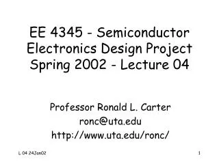
EE 4345 - Semiconductor Electronics Design Project Spring 2002 - Lecture 03 Professor Ronald L. Carter ronc@uta.edu http://www.uta.edu/ronc/
O O O O O O + + + - - - Induced E-fieldin the D.R. Ex N-contact p-contact p-type CNR n-type chg neutral reg Depletion region (DR) Exposed Donor ions Exposed Acceptor Ions W x -xpc -xp xn xnc 0
Depletion approx.charge distribution r +Qn’=qNdxn +qNd [Coul/cm2] -xp x -xpc xn xnc Charge neutrality => Qp’ + Qn’ = 0, => Naxp = Ndxn -qNa Qp’=-qNaxp [Coul/cm2]
Soln to Poisson’sEq in the D.R. Ex xn -xp x -xpc xnc -Emax
Comments on theEx and Vbi • Vbi is not measurable externally since Ex is zero at both contacts • The effect of Ex does not extend beyond the depletion region • The lever rule [Naxp=Ndxn] was obtained assuming charge neutrality. It could also be obtained by requiring Ex(x=0-dx) = Ex(x=0+dx) = Emax
Effect of V > 0 • Define an external voltage source, Va, with the +term at the p-type contact and the -term at the n-type contact • For Va > 0, the Va induced field tends to oppose Ex due to DR • For Va < 0, the Va induced field tends to add to Ex due to DR • Will consider Va < 0 now
One-sided p+n or n+p jctns • If p+n, then Na >>Nd, and NaNd/(Na +Nd) = Neff --> Nd, and W --> xn, DR is all on lightly d. side • If n+p, then Nd >>Na, and NaNd/(Na +Nd) = Neff --> Na, and W --> xp, DR is all on lightly d. side • The net effect is that Neff --> N-, (- = lightly doped side) and W --> x-
JunctionCapacitance • The junction has +Q’n=qNdxn (exposed donors), and (exposed acceptors) Q’p=-qNaxp = -Q’n, forming a parallel sheet charge capacitor.
JunctionC (cont.) • This Q ~ (Vbi-Va)1/2 is clearly non-linear, and Q is not zero at Va = 0. • Redefining the capacitance,
JunctionC (cont.) dQj = dQ’nA r +Q’n=qNdxn +qNd dQ’n=qNddxn -xp x -xpc xn xnc Charge neutrality => Q’p + Q’n = 0, => Naxp = Ndxn -qNa dQ’p=-qNadxp Q’p=-qNaxp
JunctionC (cont.) • The C-V relationship simplifies to
JunctionC (cont.) • If one plots [Cj]-2vs. Va Slope = -[(Cj0)2Vbi]-1 vertical axis intercept = [Cj0]-2 horizontal axis intercept = Vbi Cj-2 Cj0-2 Va Vbi
Practical Junctions • Junctions are formed by diffusion or implantation into a uniform concentration wafer. The profile can be approximated by a step or linear function in the region of the junction. • If a step, then previous models OK. • If not, 1/2 --> M, 1/3 < M < 1/2.
Carrier Injection and diff. ln(carrier conc) ln Na ln Nd ln ni ~Va/Vt ~Va/Vt ln ni2/Nd ln ni2/Na x xnc -xpc -xp xn 0
Ideal diodeequation • I = Is [exp(Va/nVt)-1], Is = Isn + Isp
Diffnt’l, one-sided diode conductance ID Static (steady-state) diode I-V characteristic IQ Va VQ
References * Semiconductor Physics and Devices, 2nd ed., by Neamen, Irwin, Boston, 1997. **Device Electronics for Integrated Circuits, 2nd ed., by Muller and Kamins, John Wiley, New York, 1986.