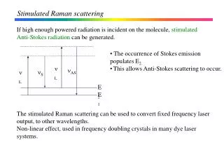
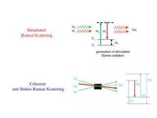
Stimulated Raman Scattering
Stimulated Raman Scattering. Coherent anti-Stokes Raman Scattering. A. Surface Enhanced Raman Scattering (SERS) as nonlinear optical effect. B. New features of the Raman spectra of single-walled carbon nanotubes highly separated into

Stimulated Raman Scattering
E N D
Presentation Transcript
Stimulated Raman Scattering Coherent anti-Stokes Raman Scattering
A. Surface Enhanced Raman Scattering (SERS) as nonlinear optical effect. B. New features of the Raman spectra of single-walled carbon nanotubes highly separated into semiconducting (99%) and metallic (98%) components. I.Baltog, M.Baibarac, L.Mihut,
Outline A • Background of Raman light scattering • Methods of amplification of the Raman emission • Surface Enhanced Raman Scattering (SERS) via plasmons excitation • SERS mechanism as a nonlinear optical process. B• Brief introductions in the Raman spectroscopy of carbon nanotubes • Abnormal Anti-Stokes SERS spectra of single-walled carbon nanotubes as single beam CARS effect . • Anti-Stokes and Stokes SERS spectra of single-walled carbon nanotubes highly separated into semiconducting (99%) and metallic (98%) nanotube components. C• Summary
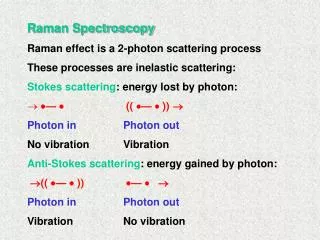
Virtual levels Electronic levels Excitation Excitation Excitation Raman anti-Stokes Excitation Raman anti-Stokes Raman Stokes Raman Stokes v3 v2 v1 v0 v3 v2 v1 v0
Raman light scattering is an complex interaction of photons and intrinsic molecular bonds E = E0cos2ltincident electromagnetic wave (laser beam) P = E = E0cos2ltinduced electric dipole moment ; is the polarizability 4 classical expression of total scattered light = o + + … ispolarizability that changes by molecular vibration;Qis coordinate that describes molecular vibration P = E = oE0cos2lt + E00 [cos2(l + )t + cos2(l - )t ] Anti-Stokes Stokes Raman scattering Both branches are amplified equally with the excitation light intensity Rayleigh scattering I(l) >> IS >> IaS 1 >> 10-6 >>10-9 Intensity Values at ~ 1500 cm-1
Information from Raman spectroscopy Characteristic Raman frequencies PbI2 ; ZnO ; CCl4 ; TiO2 C60; SWNTs; graphene Changes in frequency of Raman peak Chemical interaction; stress; strain; temperature Crystal symmetry ; orientation; antenna effect. ║ Polarization of Raman peak ┴ Morphology: crystal; mesoscopic and nanometric structures; Width of Raman peak Amount of material; film thickness; Nonlinear optical effects Intensity of Raman peak
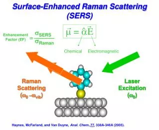
Methods of amplification of the Raman emission SERS effect chemical + plasmons Resonant excitation B.C SERS chemical 514.5 nm 676.4 nm B.V x 104 x104 -106 SERS plasmons SERS plasmons Stimulated Raman effect CARS effect ħ(2ωP – ωS) ωS ωaS = 2ωP – ωS kaS =2kP -kS ħω1 ωp ωp-ωS=Ω k(2ω0-ω1) k(ω1) x104-1010 x104-108 k(ω0) k(ω0)
Abnormal anti-Stokes SERS spectra of CuPc under resonant excitation 1 2 1 2 exc = 647.1 nm is resonant for CuPc
Surface plasmons as a channel to generate by optical pumping non-linear effects. CARS effect Single beam : I.Baltog et al. Phys. Rev. B,72,(24), 245402,(2005) J.Appl.Phys,110, 053106,(2011) Double beams Second harmonic generation Stimulated Raman effect IL >> ISωL + ☛ CARS ω = ωL± (ωL – ωS) = ωS☛ Stimulated Raman I.Baltog et al. J.Opt.Soc.Am.,13, 656,(1996) C.Steuwe, et al. Nano Lett. , 11, 5339;(2011) RL Aggarwal; et al. Appl. Spectrosc..67 , 132-135 ,(2013) J.L.Coutaz et al. Phys Rev B,32,227,(1985)
Second harmonic generation Stimulated Raman effect
s-polarization:E-field is perpendicular to the plane of incidence (German senkrecht = perpedicular) p-polarization: E-field is parallel to the plane of incidence Ez Hz E H Hy Ey Ex Hx q1 q1 e1 e1 z=0 z=0 y y e2 e2 x x q2 q2 z z Any linearly polarized radiation can be represented as a superposition of p - and s - polarization.
Boundary condition:(a) transverse component of E is conserved, (b) normal component of D is conserved creation of the polarization charges if one of the materials is metal, the electrons will respond to this polarization. This will give rise to surface plasmonmodes p-polarized incident radiation will create polarization of charges at he interface. These charges give rise to a surface plasmon modes E1z E1 H1y e1 E1x z=0 E2 E2z y e2 x H2y E2x z
Boundary condition(note that E-field has a transverse component only): transverse component of E is conserved, s-polarized incident radiation does not create polarization charges at the interface. It thus can not excite surface plasmon modes H1z H1 E1y e1 H1x z=0 H2 H2z y no polarization charges are created no surface plasmon modes are excited! e2 x E2y H2x z
condition imposed onk-vector Maxwell’s equations Surface Enhanced Raman Scattering (SERS) via plasmons excitation Charge neutrality, = 0 No direct current, j = 0Non-magnetic materials, r = 1 ( = 0) E1z E1 dielectric 1 E1x intensity x y wave propagating in x-direction localized surface mode= surface plasmon decaying into both materials z metal 2
Caracteristicileundelor de suprafata = plasmonide suprafata (SP) : • undele de suprafatarezultadinoscilatiilecolective ale electronilordinstratulmetalic; pot fi excitatenumaicuradiatiecupolarizatap(TM), care are o componenta EM perpendicularala suprafata • undele de suprafatasuntpropagativein lungulsuprafetei de separaredintredouamedii (metal-dielectric) aflate in contact; • pentru λexc= 500 nm; Lpropagare≈ 25 μm • (ii) undeevanescentepentru care amplitudineascadeexponentialcudistanta de la suprafata de separare – • pentru: λexc = 500 nm; hpenetrare ≈ 12 nmin metal si ≈ 95 nm in aer • amplitudineaundeievanescente este maxima in lungulsuprafeteilor de separare • (iv) Metale active Pb, In, Hg, Sn, Cd UVsiCu, Au, Ag VIS
dielectric e1 metall e2 prism prism Grating q1 q1 coupling gap metal metal Kretschmann-Raether geometry Otto geometry METHODS OF PLASMON EXCITATION rough surface
Experimental Material: - copper-phthalocyanine(CuPc) - SWNTs highly separated in semiconducting (99%) and metallic (98%) components Sample form : - thin films (9.5; 39; 88; 185 nm thickness ) deposited on glass and rough Au and Ag supports with different SERS activity; motivation: SERS(Au) << SERS(Ag) Measuring geometry : Backscattering under focused light ; x50 aperture objective Excitation laser light : 514.5 ; 647.1;676.4 nm ensuring non-resonant and resonant optical excitation
Abnormal anti-Stokes SERS spectra of CuPc under resonant excitation 1 2 1 2 exc = 647.1 nm is resonant for CuPc
SERS spectroscopic studies on CuPc thin films under non-resonant ( 514.5 nm) and resonant (647.1 nm) optical excitation. CARS SRS Anti-Stokes and Stokes Raman spectra of CuPcthin Films of 39 nm thickness deposited on Ag, Au and glass supports. Red curves show the anti-Stokes spectra calculated with the Boltzmann formulae applied to the corresponding Stokes Raman spectra. Anti-Stokes and Stokes Raman spectra of CuPc thin Films of 39 nm thickness deposited on Ag, Au and glass supports. Red curves show the anti-Stokes spectra calculated with the Boltzmann formulae applied to the corresponding Stokes Raman spectra.
for a Raman line at ~1500 cm-1 I(L)>> I(S)>> I(aS) 110-6 10-9 SP(L) >> SP(S) >> SP(aS) SP(L) SP(S) = SRS I(L)>> I(S)≈ I(aS) 110-6 10-6 SP(L) >> SP(S) > SP(aS) SP(L) SP(S) SRS (2SP(L) ± SP(S)) SP(aS) CARS Intensities of the anti-Stokes and Stokes Raman lines at 1530 cm-1 of 39-nm-thickCuPc films deposited on glass, Au and Ag supports. Raman measurements were performed in a backscattering geometry under non-resonant (514.5 nm) and resonant (647.1 nm) optical excitations. Data were all obtained at the same laser intensity (2 mw) focused by a 50x objective onto the surface sample. Data for each Raman branch were normalized to the intensity measured on the film deposited on a glass support. SRS
Diagrams of variations of the anti-Stokes and Stokes Raman line at 1530 cm-1 of CuPcat different excitation wavelength ( non-resonant : 514.5 and resonant : 647.1 nm), film thickness (9.5, 39 and 88 nm) and substrates used glass, Au and Ag. Intensities one each branch were normalized to the value measured on glass substrate.
Film thickness matched by plasmons wave penetration depth A2 I(L)>> I(S)≈ I(aS) 110-6 10-6 SP(L) >> SP(S) ≈ SP(aS) SRS SP(L) SP(S) CARS (2SP(L) ± SP(S)) SP(aS) Intensity of the anti-Stokes and Stokes Raman line at 1560 cm-1 of CuPcthin films of 9.5 nmthickness deposited on glass, Au and Ag supports under non-resonant (514.5 nm) and resonant (647.1 nm) laser excitation.Data were normalized to the intensity obtained on glass support.
SERS mechanism can be considered a nonlinear optical process ? • Yes, this is demonstrated by the deviations from the Boltzmann law. Plasmons coupling mechanism I(l)> I(S)> I(aS) < SPs(l) > SPs(S) > SPs(aS) mixing of surface waves (SW) SW(1) + SW(S) + SW(aS) ωmix= ωL± (ωL – ωs) ωmix= ωL- (ωL – ωs) =ωs lower frequencies are amplified at the expense of the higher frequencies Stimulated Stokes Raman effect (SRS) SRS ωmix= ωL+ (ωL – ωs) = 2ωL- ωS= ωL+ Ω=ωaS higher frequencies are amplified at the expense of the lower frequencies Coherent anti-Stokes Raman effect (CARS) CARS
Carbon allotropic particles Graphite Graphene metallic semiconductor Diamond Multi-wall carbon nanotubes Single wall carbon nanotubes Fullerene : C60
Geometry of single-walled carbon nanotube (SWNT) • d = Ch / π = 31/2aC-C(m2 + mn + n2)1/2/ π • = tan-1[31/2m/(m+2n)] N(hex/u.c) = 2(m2 + mn + n2)/d (n,m)denote the number of unit vectorsna1 si ma2 in the hexagonal honeycomblatticecontained in the vectorCh chiral angle aC-C= 1.421 Ǻ is the nearest-neighbor C-C distance in graphite n,m,define a specific SWNT: • ►Armchair(n = m, =300 ), • ►Achiral or zig-zag(n ≠ 0 or m = 0 ; = 00 ) • ►chiral (n ≠ m ≠ 0 ; 00< <300 ). • for n-m = 3k , k = 1,2,3.. Metallicproperties • for n-m ≠ 3k Semiconducting properties = 00 ; = 300 ; 0<<300
Electronic structure • - SWNT has one-dimensional (1D) electronic density of states • 1D electronic band structure derive from the 2D band structure • of the graphene honeycom sheet.
►The structure of electronic bands density of an one dimensional system (1D- carbon nanotube) derives from the bi dimensional structure (2D) of graphite ►A set of 1D energy dispersion relations is obtained by slicing up the 2D energy band structure of graphite in the circumferential direction. where a = 1.42 x Ǻ =2.46 Ǻ is lattice constant of two dimensional graphite kx and kyare the corresponding basis vectors of the reciprocal lattice; γ0 is nearest-neighbor transfer integral For an armchair SWNT tube the 1D energy dispersionrelation is: (-π < ka < π ); m = 1,.....,5 ; Similarly for a zig-zac SWNT tube: m = 1,.....,9 ; k is one dimensional vector along the tub axis ► The calculations for the electronic structure of SWNTs show that about 1/3 of the nanotubes are metallic and 2/3 are semiconducting , depending on the nanotube diameter dt and chiral angle θ. ►The metallic SWNT have a small non-vanishing 1D density of states at the Fermi level while for the semiconducting 1D SWNT the density of states is zero. ► The band gap for isolated semiconducting carbon nanotubes is proportional to the reciprocal nanotube diameter 1/dt
The tubes diameter and calculated band gap energies as function of n,m, parameters. 514.5 nm 2.4 eV 676 nm 1.83 eV 1064 nm 1.16 eV Absorption spectrum of SWNT
Electronic structure radial breathing modes RBM RBM (cm-1) = α/d (nm ) ; 223.75<α<248 • transversal axial Electronic 1D density of states for two (n,0) zig-zagnanotubes.Dotted line shows the density of states for the 2D graphene sheet (R.Saito,M.SDresselhaus et al J.Appl.Phys73,494,(1993)) -longituginal
SERS spectra of mixture semiconductor (66%) and metallic (33%) carbon nanotubes packed in bundles Stokes and anti-Stokes SERS spectra on SWNTs films of different thicknesses (h1<h2<h3, i.e about 30, 60 and 120nm ) recorded through a microscope objective of x0.55 numerical aperture under excitation wavelengths of 676.4 and 514.5 nm. The IaS/IS ratio was estimated for the G band. Au as metallic SERS support Explanation: Single beam CARS effect I.Baltog et al .PhysRev B,72,(24), 245402,(2005) SWCNTs J. Raman Spectrosc,42,303,(2011) conducting polymers J. Appl. Phys., 110, 053106, (2011) nonlinear optical materials
Abnormal anti-Stokes Raman scattering under resonant optical excitation of SWNTs is a process reminiscent to a single beam CARS effect. ICARS ~NA ωaS2d2 |χ(3)|2 I2l.IS sinc2(|Δk|.d/2) where : Il - incident pump intensity; χ(3) - the dielectric susceptibility; d - slab thickness; Δk - thephase-mismatch requirement (Δk = kas – (2 kI– kS) ; kas, kS ,kI are the wave vectors); NAis the numerical aperture of the collecting lens. a-Stokes Stokes weak temperature dependence Baltog et all. Journal of Optics A: Pure and Applied Optics 7, 1-8, (2005) ; PhysRev B,72,(24), 245402-245413,(2005);
B. Anti-Stokes and Stokes SERS spectra of single-walled carbon nanotubes highly separated into semiconducting (99%) and metallic (98%) nanotube components. B1. Absorption spectra of semiconducting (99%) and metallic (98%) SWNT 514 676 Calculated Katauraplots of van Hove singularities Energy vs. tub diameter
Breit-Wigner-Fano (B WF) profile : I=I0{1+(0 - )/}2/{1+[(0 - )/]2} = line width ; = parametre of asymetery Fano asymmetry ●The quantum interference between two configurations in the transition process into a final state with the same energy: one direct <2α2|0> and one indirect via a discrete state <2W|1> <1α1|0> , where W is a matrix element describing a nonradiative transition from discrete to continuum. ●The energy continuum of these transitions overlaps with the energy of the discrete Raman active optical phonon of the same symmetry and an interference between the phonon and the electronic transition takes place. M.A.Pimenta, …,G.Dresselhaus, and M.S.Dresselhaus.., Phys.Rev.B 58,R16016-R16019,(1998)
TO LO Stokes and anti-Stokes Raman spectra for SWNT’s of d~1.49 nm taken at four different values of E laser LO TO S. D. M. Brown et al. Phys. Rev. B 61, R5137(2000) Raman G+ and G- peaks associated to LO andTO phonons for semiconducting and metallic SWNTs ? S. Piscanec et al. Phys. Rev. B 75, 035427(2007)
Since metals are infinitely polarizable, it is hard to see how a vibration of the atoms • in the crystal lattice could cause a change in the polarizability. • Raman activity of metals may be generated by small clusters of metal atoms, and in • the case of metallic nanotubes by their association in bundles • Fano Raman profile The relative BWF intensity is always weak for thin bundles or individual tubes but varies for thicker bundles. The solid lines show estimated relative intensities for pure metallic bundles and bundles containing isolated or noninteracting metallic tubes. K.Kempa et al.Phys Rev B 66, 161404 (2002); 66, 195406 (2002)
G Raman band profiles of metallic ( 98%) and semiconductor (99%) carbon nanotubes Supports: glass ; Au; Ag Anti-Stokes (a1;b1) and Stokes (a2;b2) G Raman band profiles of metallic (~98% pure, a1;a2) and semiconductor (~99% pure, b1;b2) SWNTS deposited in a thin layer on glass (black), Au (red) and Ag (blue) supports. All spectra were recorded in a backscattering geometry with 2 mW of laser intensity focused on the sample through a 50x objective.
SERS evidence of anomalous behavior in anti-Stokes Raman branch of metallic nanotubes. Stimulated Raman Scattering effect CARS effect Intensities of the anti-Stokes and Stokes G Raman lines (1595 cm-1) under 514.5; 647.1 and 676.4 nm excitation light (normalized by the intensity obtained from samples with the glass substrate) for metallic (M, ~98 % pure) and semiconductor (S, ~99% pure) C-SWNT thin films deposited on glass, Au and Ag supports. The intensity of the laser light focused on all samples was 2 mW.
Supports: glass Au Ag MWNT LAUSANNE Metallic MWNT ALDRICH Metallic + Semiconductor
Insulator, semiconductor and metal Clasification based on bandstructure Conduction band Conduction band EF Eg Vibration levels Energy Valence band INSULATOR or SEMICONDUCTOR METAL
Absorption: Semiconductors Energy of electron unfilled states I o filled states • Absorption by electron transition occurs if hn > Egap incident photon energy hn Egap typical resonance
Optical Properties of Metals: Absorption Energy of electron unfilled states Incident photon DE = h required covers a large spectral range ; no typical resonance I o filled states of energy • Absorption of photons by electron transition: h • Metals have a fine succession of energy states that causes absorption and reflection; • Normally, the Raman activity is conditioned of the vibrations which change the poalarizability of the molecule or material. • Because the visible light cannot penetrate the metals , Raman scattering results from the modulation of the electronic susceptibility by the optical vibration modes within the skin depth by the optical vibration modes . • Inside the medium, the amplitude of the electric field decays to zero rapidly with distance.
Variation with excitation laser intensity and temperature of the anti-Stokes Raman G band of semiconductor and metallic carbon nanotubes Typical non-linear dependence for a non-linear optical process SRS Intensities of Stokes (filled symbols) and anti-Stokes (open symbols) Raman lines at 1595 cm-1 (G band) measured in a backscattering geometry for semiconducting (~99% pure; up triangles) and metallic (~98% pure; down triangles) of C-SWNTs under 676.4 nm excitation light focused through a 50x microscope objective. The samples were in the form of thin films layered on a glass (triangles) substrate or Ag SERS supports (stars). The Raman intensity was normalized to the signal measured at the lowest excitation intensity (0.2 mW). Variation with temperature of the IaS/IS ratio associated with the Raman G band (1590 cm-1) for semiconducting (~99% pure, red symbols) and metallic (~98% pure, blue symbols) of C-SWNTs deposited on a glass substrate. All data were obtained at exc = 676.4 nm with 2 mW of laser power focused on the sample through a 50x microscope objective. The green line illustrates the variation allowed by applying the Boltzmann law to the recorded Stokes Raman spectra for metallic tubes.
Polarized Raman spectra of isolated semiconducting and metallic nanotubes Anti-Stokes Raman intensity of the Raman G band for semiconductor (~99% pure; a) and metallic (~98% pure; b) SWNTs on a Ag support versus the intensity of excitation laser light. All data were obtained at exc = 676.4 nm with light polarized along (LO) and perpendicular (TO) to the tubes’ axes. Anti-Stokes and Stokes Raman spectra for semiconductor (~99% pure; S1,S2; black curve) and metallic (~98% pure; M1,M2; red curve) C-SWNTs excited at exc = 676.4 nm with light polarized along (LO) and perpendicular (TO) to the tubes’ axes.
Conclusion: i) SERS effect manifests differently under non-resonant and resonant optical excitations, it results from the coupling of plasmons associated with the incident light with the plasmons associated with the Stokes and anti-Stokes spontaneous Raman emissions. ii) Under non-resonant and resonant optical excitation SERS manifests as stimulated Raman process and CARS effect, respectively. iii) Contrary to the results reported so far , and regardless of whether the optical excitation was non-resonant or resonant and regardless of whether glass, Au or Ag was used as the substrate, the metallic single wall carbon nanotubes (SWNTs) do not show an anomalous anti-Stokes Raman emission. iv)Semiconducting SWNTs always show an anomalous anti-Stokes Raman emission that grows further under increases in the excitation light intensity or temperature. v) Semiconducting SWNTs behave differently than metallic SWNTs because of the splitting of electronic levels into a vibration structure, which under resonant optical excitation changes the polarizability of the material by overpopulating the states and contributes to an enhancement of the anti-Stokes Raman emission; vi) Metallic SWNTs (like any metal) are infinitely polarizable at very short distances, fact which determines the invariance of the Stokes Raman spectrum under changes of the polarization of the excitation light
Own contributions: ApplPhysLett 66,1187-1190,(1995) J Opt Soc Am B 13, 656-660, (1996) Pure Appl. Opt. 5 , 645–653,(1996) J. Raman Spectrosc. 29, 825È832 (1998) Phys Rev B 65, 235401,(2002) Carbon, 40,2201-2211,(2002) J. Opt. A: Pure Appl. Opt. 7,632–639,(2005) Phys. Rev. B,72,(24), 245402-245413,(2005) Carbon, 43,1-9,(2005) J Raman Spectrosc 36,676-698, (2005) PhysicaE: 40(7),2380,(2008) J. Phys:CondensedMatter. 20,(27), 275215, (2008) Physicastatus solidi (b) 245, (10), 2221, (2008) Carbon ,47, (5),1389-1398,(2009) Synthetic Metals 159 , 2173,(2009) J Raman Spectrosc,42,(3),303, (2011 ) J. Phys. B: At. Mol. Opt. Phys. 44,095401, (2011) Optical materials, 33, (9), 1410,(2011) J ApplPhy, 110, 053106, (2011) Proc. Romanian Acad., Series A, 13, (2), 109–117, (2012) J Phys Chem. C, 116, 25537−25545, (2012) Optics Communication : submitted, (2013) J Raman Spectrosc, submitted, 2013 Journal of Optics : submitted, (2013)
WEB of Science 2000-2012 9,089 records.Topic = (Raman carbon nanotubes)
Carbon allotropic particles Graphite Graphene metallic semiconductor Diamond Multi-wall carbon nanotubes Single wall carbon nanotubes metallic Fullerene : C60
substitute kx The surface plasmone mode always lies beyond the light line, that is it has greater momentum than a free photon of the same frequency light cone = c k w k What is the wavelength of the surface plasmon ? let us find k: