Crystal-Air surface
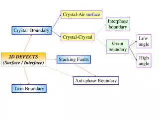
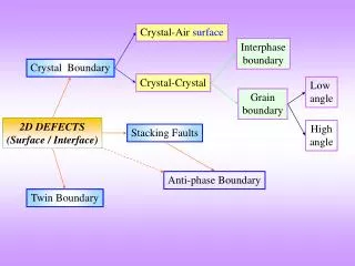
2D DEFECTS (Surface / Interface). Anti-phase Boundary. Crystal-Air surface. Interphase boundary. Crystal Boundary. Crystal-Crystal. Low angle. Grain boundary. High angle. Stacking Faults. Twin Boundary. 2D DEFECTS (Surface / Interface). Anti-phase Boundary. Alternate view.

Crystal-Air surface
E N D
Presentation Transcript
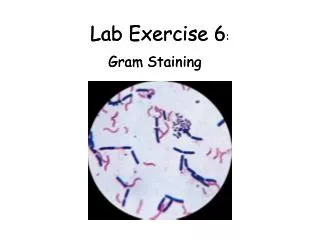
2D DEFECTS(Surface / Interface) Anti-phase Boundary Crystal-Air surface Interphaseboundary Crystal Boundary Crystal-Crystal Low angle Grainboundary Highangle Stacking Faults Twin Boundary
2D DEFECTS(Surface / Interface) Anti-phase Boundary Alternate view Low angle External Grain boundary Highangle Rotation Homophase Twin Boundary Mirror Internal Stacking Faults Translation Heteropase (From lecture notes of Dr. Rajesh Prasad)
Low angle High angle Based on angle of rotation Twist Homophase Tilt Based on axis Mixed Based on Lattice Models Special CSL Random Based on Geometryof the Boundary plane Curved Faceted Mixed
Coherent Heteropase Semi-coherent Incoherent
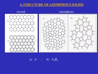
Surface Imperfections • 2D in a mathematical sense • The region of distortion is ~ few atomic diameters in thickness
External surface of the crystal • External surfaces have energy related to the number of bonds broken at the surface No. of atoms/ unit area Surface Energy/unit area (J/m2) No. of bonds broken/ unit area Bond energy / bond As two surfaces are created / bond broken
Interphaseboundary Grainboundary
Grain Boundary • The grain boundary region may be distorted with atoms belonging to neither crystal • The thickness may be of the order of few atomic diameters • The crystal orientation changes abruptly at the grain boundary • In an low angle boundary the orientation difference is < 10º • In the low angle boundary the distortion is not so drastic as the high-angle boundary → can be described as an array of dislocations • Grain boundary energy is responsible for grain growth on heating ~ (>0.5Tm) • Large grains grow at the expense of smaller ones • The average no. of nearest neighbours for an atom in the grain boundary of a close packed crystal is 11
Low angle grain boundaries (misorientation < 10º) Two extremes TILT An array of edge dislocations TWIST An array of screw dislocations • Rotation axis lies on the boundary plane • Rotation axis lies to the boundary plane
b 2h Book
No visible Grain Boundary 2.761 Å Fourier filtered image Dislocation structures at the Grain boundary ~8º TILT BOUNDARY IN SrTiO3 POLYCRYSTAL
Twin Boundary • The atomic arrangement on one side of the twin boundary is related to the other side by a symmetry operation (usually a mirror) • Twin boundaries usually occur in pairs such that the orientation difference introduced by one is restored by the other • The region between the regions is called the twinned region Annealing twins (formed during recrystallization) Twin Deformation twins (formed during plastic deformation)
Twin boundary in Fe doped SrTiO3 bicrystals (artificially prepared) High-resolution micrograph Mirror related variants Twin plane [1] S. Hutt, O. Kienzle, F. Ernst and M. Rühle, Z Metallkd, 92 (2001) 2
Stacking Fault • Error in the sequence of stacking atomic planes → Stacking fault • Defined by a shift vector …ABC ABC ABC ABC… FCC stacking FCC stacking with a stacking fault …ABC AB AB ABC… Thin region of HCP type of stacking • In above the number of nearest neighbours remains the same but next-nearest neighbours are different than that in FCC • Stacking fault energy ~ 0.01 – 0.05 J/m2 • Stacking fault in HCP can lead to thin region of FCC kind of stacking