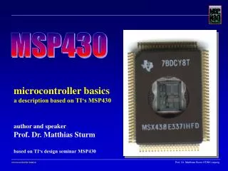
The Texas Instruments MSP430
The Texas Instruments MSP430. Block diagram. The Outside View—Pin-Out. The pin-out shows which interior functions are connected to each pin of the package. D ual-in-line package (PDIP) with pins 0 . 1 inch apart .


The Texas Instruments MSP430
E N D
Presentation Transcript
The Outside View—Pin-Out • The pin-out shows which interior functions are connected to each pin of the package. • Dual-in-linepackage (PDIP) with pins 0.1 inch apart. • A general warning: Packages with the same shape do notalways have the same pin-out.
The Outside View—Pin-Out • The most obvious feature is that almost all pins have several functions. • Silicon is cheap but pins are expensive. • VCC and VSS are the supply voltage and ground for the whole device (the analogand digital supplies are separate in the 16-pin package). • P1.0–P1.7, P2.6, and P2.7 are for digital input and output, grouped into ports P1 and P2. • TACLK, TA0, and TA1 are associated with Timer_A; TACLK can be used as theclock input to the timer, while TA0 and TA1 can be either inputs or outputs. Thesecan be used on several pins because of the importance of the timer. • A0−, A0+, and so on, up to A4±, are inputs to the analog-to-digital converter. VREF is the reference voltage for the converter. • ACLK and SMCLK are outputs for the microcontroller’s clock signals. These canbe used to supply a clock to external components or for diagnostic purposes
The Outside View—Pin-Out • SCLK, SDOare used for the universal serial interface, whichcommunicates with external devices using the serial peripheral interface (SPI) or inter-integrated circuit (I2C) bus. • XIN and XOUT are the connections for a crystal, which can be used to provide an accurate, stable clock frequency. • RST is an active low reset signal. Active low means that it remains high near VCCfor normal operation and is brought low near VSS to reset the chip. Alternativenotations to show the active low nature are _RST and /RST. • NMI is the nonmaskable interrupt input, which allows an external signal tointerrupt the normal operation of the program.
The Inside View—Functional Block Diagram • On the left is the CPU and its supporting hardware, including the clock generator.The JTAG interface is used to communicate with adesktop computer when downloading a program and for debugging.
The Inside View—Functional Block Diagram • The main blocks are linked by the memory address bus (MAB) and memory databus (MDB). • These devices have flash memory, and128 bytes of RAM. • All MSP430s include input/output ports, Timer_A, and a watchdog timer. The universal serial interface (USI) and sigma–deltaanalog-to-digital converter (SD16_A) are particular features of this device. • The brownout protection comes into action if the supply voltage drops to adangerous level. • There are ground and power supply connections. Ground is labeled VSS and istaken to define 0V. The supply connection is VCC. The performance of the devicedepends on VCC. For example, it is unable to program the flash memory ifVCC < 2.2V and the maximum clock frequency of 16MHz is available only ifVCC ≥ 3.3V.
Memory • Thememory address bus is 16 bits wide so there are 216 = 65,536 = 64K = 0x10000addresses. The first address is 0, so the range is 0x0000 to 0xFFFF • 0 is a valid address(it is the Interrupt Enable 1 register, IE1). • The memory data bus is 16 bits wide and can transfer either a word of 16 bits or a byte of8 bits. Bytes may be accessed at any address but words need more care. • The address of aword is defined to be the address of the byte with the lower address, which must be even. • Thus the two bytes at 0x0200 and 0x0201 can be considered as a valid word with address0x0200, which may be fetched in a single cycle of the bus. • An important case is that instructions are composed ofwords and must therefore lie on even addresses.
Memory • Ordering of bits, bytes, and words in memory. Suppose that a word contains the hexadecimal value 0x1234.
Memory • Little-endian ordering: The low-order byte is stored at the lower address and thehigh-order byte at the higher address. This is used by the MSP430 and is the morecommon format. • Big-endian ordering: The high-order byte is stored at the lower address. This is usedby the Freescale HCS08, for instance.
Memory Map Here is a brief description of each region: • Special function registers: Mostly concerned with enabling functions of somemodules and enabling and signalling interrupts from peripherals. • Peripheral registers with byte access and peripheral registers with word access:Provide the main communication between the CPU and peripherals. Some must beaccessed as words and others as bytes. They are grouped in this way to avoid wastingaddresses. If the bytes and words were mixed, numerous unused bytes would be neededto ensure that the words were correctly aligned on even addresses.
Memory Map • Memory map of the MSP430F2013, based on the data sheet and theMSP430x2xx Family User’s Guide.
Memory Map • Random access memory: Used for variables. This always starts at address 0x0200 andthe upper limit depends on the size of the RAM. • Bootstrap loader: Contains a program to communicate using a standard serialprotocol, often with the COM port of a PC. • Information memory: A 256B block of flash memory that is intended for storage ofnonvolatile data. • Code memory: Holds the program, including the executable code itself and anyconstant data. • Interrupt and reset vectors: Used to handle “exceptions,” when normal operation ofthe processor is interrupted or when the device is reset. • The range of addresses has been extended from 64KB to 1MB in the MSP430X.
Central Processing Unit • The central processing unit (CPU) executes the instructions stored in memory. It includes thearithmetic logic unit (ALU), which performs computation, a set of 16 registers designatedR0–R15 and the logic needed to decode the instructions and implement them. • The CPUcan run at a maximum clock frequency fMCLK of 16MHz in the MSP430F2xx family andsome newer MSP430x4xx devices, and 8MHz in the others. • The CPU can be stoppedand will retain its state until it is restarted. This is essential for low-power operation to bestraightforward. • The first fourregisters have dedicated functions with alternative names, while the remaining 12 R4–R15are working registers for general purposes. Either words or bytes can be written to theCPU registers but the behavior for bytes is different from main memory: The destination isalways the low byte and the high byte is cleared (reset to 0).
Central Processing Unit • The generous set of 16 registers is characteristic of a reduced instruction set computer(RISC). • Program counter, PC: This contains the address of the next instruction to be executed,“points to” the instruction in the usual jargon. Instructions are composed of 1–3 words,which must be aligned to even addresses, so the lsb of the PC is hard-wired to 0.
Central Processing Unit • Stack pointer, SP: When a subroutine is called, the CPU jumps to the subroutine,executes the code there, then returns to the instruction after the call. It must thereforekeep track of the contents of the PC before jumping to the subroutine, so that it canreturn afterward. This is the primary purpose of the stack. The stack pointer holds the address of the most recently added word and isautomatically adjusted as the stack grows downward in memory or shrinks upward. • Status register, SR: This contains a set of flags (single bits), whose functions fallinto three categories. The most commonly used flags are C, Z, N, and V. The Z flag is setif the result was zero and cleared if it was nonzero, for instance. Decisions that affectthe flow of control in the program can be made by testing these bits.Setting the GIE bit enables maskable interrupts.The final group of bits is CPUOFF, OSCOFF, SCG0, and SCG1, which control themode of operation of the MCU. All systems are active when all bits are clear. Settingvarious combinations of these bits puts the MCU into one of its low-power modes.
Central Processing Unit • Constant generator: This provides the six most frequently used values so that theyneed not be fetched from memory whenever they are needed. It uses both R2 and R3 toprovide a range of useful values by exploiting the CPU’s addressing modes. • General purpose registers: The remaining 12 registers, R4–R15, are general workingregisters. They may be used for either data or addresses because both are 16-bit values.
Memory-Mapped Input and Output • Simple digital input and output takes place through sets of pins on the package of theintegrated circuit called ports. • Each port has up to 8 pins although not all may be availablein a particular package. TI usesnumbers and the ports are called P1, P2, and so on (there is no P0 in current devices). • Typical pins can be configured for either input or output and some inputs may generateinterrupts when the voltage on the pin changes. This is useful to awaken a system that hasentered a low-power mode while it waits for input from a (slow) human. • The ports simply appear to the CPU as particular memoryregisters called peripheral registers. • Each port is associated with a byte and each bitcorresponds to a pin on the package (if implemented). These registers can be read, written,and modified in almost the same way as simple registers in RAM. You can even doarithmetic with them, with some restrictions. For example, you simply read the registerP1IN in the usual way to find the logical values on the inputs to port P1. Input voltagesnear ground, VSS, give a logical 0 while voltages near the supply, VCC, give a logical 1.
Memory-Mapped Input and Output • Port P1 input, P1IN: Reading returns the logical values on the inputs if they areconfigured for digital input and output. This register is read-only. It is also volatile,which means that it may change at a time that a program cannot predict. This is ofcourse why the input port is there, so that the MCU can react to its surroundings. Youwant to know when a user presses a button, for instance. This is a reminder that P1IN isnot just a simple memory and that some care is needed when programming in C. • Port P1 output, P1OUT:Writing sends the value to be driven onto the pin if it isconfigured as a digital output. If the pin is not currently an output, the value is stored ina buffer and appears on the pin if it is later switched to be an output. • Port P1 direction, P1DIR: A bit of 0 configures the pin as an input, which is thedefault.Writing a 1 switches the pin to become an output.
Other Peripherals • Clock Generator • Basically the clock signal is a square wave whose edges trigger hardware throughout thedevice so that the changes in different components are synchronized. In manyapplications the MCU spends most of its time in a low-power mode until some eventoccurs, when it must wake up and handle the event rapidly. It is often necessary to keeptrack of real time, either so that the MCU can wake periodically or to time-stamp external events. Therefore, two clocks with quite differentspecifications are often needed.
Clock Generator • Crystal: Accurate and stable (does not change greatly with time or temperature). Crystals formicrocontrollers typically run at either a high frequency of a few MHz to drive the mainbus or a low frequency of 32,768 Hz for a real-time clock. The disadvantages are thatcrystals are expensive and delicate.Crystal oscillators also take a long time to start up and stabilize,often around 105 cycles, which is an unavoidable side effect of their high stability. • Resistor and capacitor (RC): Cheap and quick to start but used to have poor accuracyand stability. The components can be external but are now more likely to be integratedwithin the MCU.
Clock Generator • There are internal clocks, which are the same in all devices: • Master clock, MCLK, is used by the CPU and a few peripherals. • Subsystem master clock, SMCLK, is distributed to peripherals. • Auxiliary clock, ACLK, is also distributed to peripherals.
Clock Generator • ACLK comes from a low-frequency crystal oscillator, typically at 32 KHz. • Both MCLK and SMCLK are supplied by an internal digitally controlled oscillator(DCO),which runs at about . • Note that ACLK requires an external crystal, which is supplied on most demonstrationboards but not TI’s basic development kits. No crystal meansno ACLK with most MSP430s. However, devices in the MSP430F2xx family (exceptthe F21x1, which were first to be introduced) include an internal, very low-power,low-frequency oscillator (VLO) that can be selected for ACLK if there is no crystal. • One of the most important characteristics of the DCO is that it starts very rapidly at fullspeed, taking less than 1microsecondin the MSP430F2xx. This is a critical feature for a low-powersystem.
Exceptions: Interrupts and Resets • Execution of a program usually proceeds predictably, but there are two classes ofexception to this rule: interrupts and resets: • Interrupts: Usually generated by hardware (although they can be initiated by software)and often indicate that an event has occurred that needs an urgent response. The processor stops what it was doing, stores enough information (thecontents of the program counter and status register) for it to resume later on andexecutes an interrupt service routine (ISR). It returns to its previous activity when theISR has been completed. Thus an ISR is something like a subroutine called by hardware(at an unpredictable time) rather than software. A second use of interrupts, which isparticularly important in the MSP430, is to wake the processor from a low-power state. • Resets: Again usually generated by hardware, either when power is applied or whensomething catastrophic has happened and normal operation cannot continue. This canhappen accidentally if the watchdog timer has not been disabled, which is easy toforget. A reset causes the device to (re)start from a well-defined state.
Exceptions: Interrupts and Resets • The CPU must be told where to fetch the next instruction following an interrupt or reset.The address of this instruction is called a vector and can be specified in different ways. Thesimplest is to have a single vector for resets and another for all interrupts. • The MSP430 uses vectored interrupts. Each ISR has its own vector, which isstored at a predefined address in a vector table at the end of the program memory(addresses 0xFFC0–0xFFFF).
Exceptions: Interrupts and Resets • The same method is used for a reset, whose vector is stored in the very last word ofmemory at 0xFFFE.
Data Sheet • Front page: Gives a brief overall description. • Device pin-out: Shows the style of packages and their connections. • Functional block diagram: Shows the main systems within the integrated circuit. • Terminal functions: Show what peripherals. • Short-form description: Gives a brief summary of the CPU, instruction set, operating(low-power) modes, and interrupt vector addresses. • Special function registers: Mainly control interrupts. • Memory organization: Gives the main features of the memory map.
Principles for low power applications: • Maximize the time in standby, • Use interrupts to control program flow, • Manage the power of internal peripherals, • Effective code is a must.
volatile: • Used if an event outside the program can change the content of a variable, for example an ADC; • A statement using this descriptor informs the compiler that this variable should not be optimized.