MSP430
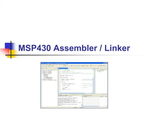
MSP430. More on MSP430. CodeComposer. TI recently launched Code Composer Essentials v3. This IDE’s latest version (version 3) supports all available MSP430 devices. The new features of CCE v3 include: - Free 16 kB code-limited version; - Supports the large memory model (Place data >64k);


MSP430
E N D
Presentation Transcript
MSP430 More on MSP430
CodeComposer TI recently launched Code Composer Essentials v3. This IDE’s latest version (version 3) supports all available MSP430 devices. The new features of CCE v3 include: - Free 16 kB code-limited version; - Supports the large memory model (Place data >64k); - Enhanced Compatibility with IAR C-code: - #pragma (ISR declarations), most intrinsics. - GDB Debugger replaced by TI proprietary debugger that allows faster single stepping; - Hardware Multiplier libraries (16-bit and 32-bit multiplies); - CCE v2 project support (auto convert); - Breakpoints: - Extended Emulation Module (EEM) support via unified breakpoint manager; - Using of EEM (predefined Use Cases); - Unlimited Breakpoints
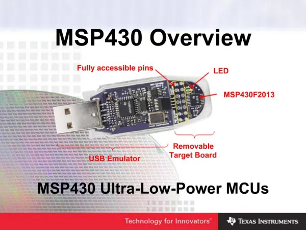
MSP-EXP430FG4618 The MSP430FG4618/F2013 experimenter’s board is based on the Texas Instruments ultra-low power MSP430 family of microcontrollers [1, 2]. Residing on this board are the MSP430FG4618 [3] and the MSP430F2013 [4] microcontrollers.
An MSP430 Flash Emulation Tool (MSP-FET430UIF) is required to download code and debug the MSP430FG4618 and MSP430F2013. Two separate JTAG headers are available, supporting independent debug environments. MSP430FG4618 uses the standard 4-wire JTAG connection while the MSP430F2013 uses the Spy-Bi-wire (2-wire) JTAG interface allowing all port pins to be used during debug.
Wireless communication is possible through the expansion header which is compatible with all Chipcon Wireless Evaluation Modules from Texas Instruments. Interface to a 4-mux LCD, UART connection, microphone, audio output jack, buzzer, and single touch capacitive touch pad enable the development of a variety of applications. Communication between the two on-board microcontrollers is also possible. In addition, all pins of the MSP430FG4618 are made available either via headers or interfaces for easy debugging.
Power may be provided locally from two on-board AAA batteries, externally from aFlash emulation tool (FET), or an external supply. The power source is selectedby configuring jumpers VCC_1, VCC_2, and BATT. PWR1 and PWR2 will supplypower to each MSP430 independently. The battery jumper BATT is used to select the on-board batteries to power thesystem, independent of the FET connections. The user must ensure that thisvoltage meets the requirement for proper functionality of the MSP430.
The power selection jumpers VCC_1 and VCC_2 select the power connectionsbetween the board and each FET interface. These jumpers are two rows of 3-pinheaders, one for each MSP430 on-board. VCC_1, the bottom row, is for theMSP430FG4618 and, VCC_2 on the top row, is for the MSP430F2013. A jumperplaced on the rightmost 2-pins (FET) selects the JTAG FET as the power source. A jumper placed on the leftmost 2-pins (LCL) would enable local power (eitherfrom the batteries or an external supply) to be applied to each FET for proper logicthreshold level matching during program/debug.
Headers PWR1 and PWR2 have been provided to enable power to the individualMSP430s. A jumper placed on PWR1 provides power to the MSP430FG4618 anda jumper placed on PWR2 provides power to the MSP430F2013. Individual devicecurrent consumption can be measured via each of these jumpers. Once the required power selections have been made the experimenter’s board isready to be used. Both the MSP430FG4618 and MSP430F2013 are factoryprogrammed. After power up, the MSP430FG4618 executes an ultra-low powerreal-time clock displayed on the LCD
Some of these interfaces have the option of being inactive when not in use to conserve power. This is made possible by MSP430 port pin configurations and/orhardware jumpers on-board. 4-Mux LCD Display The integrated SoftBaugh SBLCDA4 LCD display supports 4-MUXoperation and interfaces to the LCD driver peripheral of theMSP430FG4618. More information on the LCD can be obtained from the manufacturer’s datasheet. Momentary-On Push Buttons Two external push buttons, S1 and S2, are connected to the interruptcapable MSP430FG4618 digital I/O port, P1. Light Emitting Diodes (LEDs) The experimenter board has a total of four LEDs, three connected to theMSP430FG4618 and one connected to the MSP430F2013. The LEDs areprimarily used for display purposes. Two of the LEDs can be disconnectedusing jumpers to reduce the overall power consumption of the board. Buzzer A buzzer is connected to a digital I/O port of the MSP430FG4618. It isdriven via a port pin of the MSP430. The buzzer can be completelydisconnected by using jumper JP1. Single-Touch Sensing Interface A capacitive touch sensing interface in the shape of a “4” is provided onboard.This touchpad is connected to the digital I/O ports of theMSP430F2013. A total of 16 individual segments form the touchpad, andactivity is monitored by the MSP430F2013. The resulting data iscommunicated to the MSP430FG4618 via the MSP430 intercommunicationconnections provided on-board.
Communication Peripherals Chipcon Wireless Evaluation Module Interface Interface to the wireless world is accomplished via the Wireless EvaluationModule header supporting the CCxxxxEMK boards from TI. Thetransceiver modules are connected to the USART of the MSP430FG4618configured in SPI mode. Libraries [6] that interface the MSP430 to thesetransceivers are available at www.ti.com/msp430. The CC2420EMKsupports the 802.15.4/Zigbee standard. The CC1100EMK may beconfigured to work at an RF carrier frequency of up to 868 MHz and theCC2500EMK/CC2420EMK at an RF carrier frequency of 2.4 GHz. RS-232 For a serial interface to a PC, the MSP430FG4618 supports the standardRS-232 9-pin interface via its USCI peripheral configured in UART mode. Standard baud rates for transmission and reception can be configuredusing in software I2C/SPI The MSP430FG4618 and the MSP430F2013 have support for I2C andSPI protocols using the USCI and the USI peripherals. This protocol isused for inter-processor communication The link can be disconnected inhardware allowing these peripherals to be used for other communicationpurposes.
Analog Signal Chain The experimenter’s board is capable of forming a complete analog signal chainusing the MSP430FG4618. This board can be used for numerous audioapplications and is capable of recording and playback of audio signals without theuse of additional external components.
Microphone The microphone is connected to the MSP430FG4618 and may be used for various applications. The microphone is enabled/disabled via a port pinconnected to the MSP430FG4618. An active first order high-pass filter (HPF) with a cut-off frequency set atapproximately 340Hz follows the microphone to eliminate extremely lowinput frequencies. An optional 2nd order Sallen-Key active low-pass filter(LPF) with a cut-off frequency set to approximately 4 kHz removes thehigh-frequency noise on the analog output of the 12-bit DAC.
Analog Output Analog output can be brought out of the board via a mono 3.5mm jack connected to the integrated Op-Amp OA2. The input to this amplifier can be internally connected to the DAC12 output of the MSP430FG4618. Several attenuation options are provided internally and in hardware using jumper JP4.
System Clocks The experimenter’s board has various system clock options that support low andhigh frequencies. Each MSP430 has integrated clock sources as well as supportfor external connections. MSP430F2013 Clock Sources The MSP430F2013 uses the internal VLO operating at ~12kHz for anultra-low power standby wake up time base. The integrated DCO isinternally programmable at frequencies up to 16MHz for high speed CPUand system clocking. MSP430FG4618 Clock Sources A standard 32.768kHz watch crystal is populated at footprint X2 andsources source ACLK of the MSP430FG4618 for low frequency, ultra-lowpower standby operation and RTC functionality. The integrated FLL+ clockmodule provides a programmable internal high frequency clock source forthe CPU and other peripherals on-chip. In addition to the FLL+, anexternal high frequency crystal or resonator up to 8MHz can be added viafootprint X1.
Procedure By analysis of the schematics, we need to determine which I/O port pin is connected to the LED on the board: - Consult the MSP430FG4618/F2013 Experimenter’s Board User's Guide slau213a.pdf - LED1 is connected to Port 2.2 - Consult the eZ430-F2013 Development Tool User's Guide slau176b.pdf - LED1 is connected to Port 1.1 - Consult the eZ430-RF2500 Development Tool User's Guide slau227c.pdf - LED is connected to Port 1.0
Include the standard register and bit definitions for the TI MSP430 microcontroller device (example for the SP430FG18/MSP430F2013 Experimenter's board): #include <msp430xG46x.h> Define the main routine: void main (void){ The watchdog timer must be prevented from generating a PUC. Write 0x5A to the eight MSBs of the Watchdog timer control register, WDTCTL: WDTCTL = WDTHOLD | WDTPW; Port control registers: - Set the LED port pin as an output; P2DIR: Port 2.2 is set as an output: P2DIR |= 0x04; // to force the pin setting. It is uses an OR operation ( | ) with P2DIR and 0x04
Use an infinite loop to modify the state of the port; Use a software delay loop to generate the pause interval. (a long software delay loop is used here for simplicity - in real applications, a timer would be used) - Because no clock is defined, the device will use the 32.768 kHz watch crystal. In order for a rate of one blinking LED state transition each second, the software delay loop should count to approximately 30000 {30000/32768 = +/- 1 sec}; volatile unsigned int i; while(1) { //Infinite loop i=30000; //Delay do (i--); while (i !=0); // Port control registers inside the loop: // P2OUT: To switch the port state between low and // high state during program execution: P2OUT ^= 0x04; } } // It uses an XOR operation ( ^ ) between P2OUT and 0x04:
Toggle the LED state by pressing the push button • Button S1 is connected to Port 1.0; Ports control registers: - Set push button pin port as an input - P1DIR: Port 1.0 is set as an input: P1DIR &= ~0x01 // to force the pin setting to 0. It is uses an AND operation ( & ) between P1DIR and 0xFE - Enable interrupts to this pin port; - P1IE: Enable interrupt to port 1.0: P1IE |= 0x01; // Interrupt Enable in P1.0 - PIIES: Call the port interrupt on a high-to-low transition: P1IES |= 0x01; // P1.0 Interrupt flag high-to-low transition - Configure the watchdog timer to prevent a PUC during the program execution; WDTCTL = WDTPW | WDTHOLD; //Stop Watchdog Timer - Enable Global Interrupts and configure low power mode 3; _BIS_SR (LPM3_bits + GIE); //Low Power Mode with interrupts enabled - Create a interrupt service routine, that includes: - Toggle LED1 pin port; - Delay for button debounce; - Clear interrupt flag.
#pragma vector=PORT1_VECTOR __interrupt void Port_1 (void) { volatile unsigned int i; P2OUT ^= 0x04; // Toggle Port P2.2 i=1500; // Delay, button debounce do (i--); while (i !=0); while (! (P1IN & 0x01)); // Wait for the release of the button i=1500; // Delay, button debounce do (i--); while (i !=0); P1IFG & = ~0x01; // Clean P1.0 Interrupt Flag }
Homework2 • Write a code to work with MSP430 • Enable/disable LED blinking by push button press by: • Detect of the button is pressed: • Include a control flow program variable that detects if the LED is blinking or not, when the button is pressed: • Define a variable that indicates whether the LED is blinking; • Set the program flow depending on the state of the variable.
Timers • Introduction • Correct system timing is a fundamental requirement for the proper operation of a real-time application. • The timing definition can dictate how the data information processed during the execution of the application program. • The clock implementations vary between devices in the MSP430 family. Each device provides different clock sources, controls and uses. • The MSP430 4xx family has two general-purpose 16-bit or 8-bit counters and event timers, named Timer_A, Timer_B, and a Basic Timer. • The timers may receive an internal or external clock. Timer_A and Timer_B also include multiple independent capture and compare blocks, with interrupt capabilities.
Example • This example implements a memory clock using the features provided by Timer1. The clock is updated once every second by the Basic Timer1 interrupt service routine (ISR). This procedure also performs switching of LED1. In order to evaluate the execution time of the routine, LED2 is kept active during the execution of the ISR. When the ISR has completed, the device goes into low power mode, until the new interrupt wakes it up.
Example This application sets Basic Timer1 to generate an interrupt once every second. The interrupt service routine generated by this peripheral is required to update the clock stored in memory. Moreover, it must refresh the content of the clock displayed on the LCD. Thus, the system resources used by this application are: - Basic Timer1; - I/O ports; - LCD; - Interrupts; - Low power modes.
Software application organization The first task is to disable the Watchdog Timer. It should be stated that this feature, when used correctly, makes the application more robust. The resources needed for the LCD are all configured. The memory clock consists of setting three global variables: hour, min, and sec, all of the type unsigned char, used to store the hours, minutes and seconds values elapsed respectively since the beginning of the execution of the application. These variables are initialized with zero values. The LCD is refreshed at startup to show the initial clock value. LED1 is used as an indicator of Basic Timer1 ISR execution. The execution time can be determined through it. In addition, LED2 state switches whenever the Basic Timer1 ISR is executed. The Basic Timer1 is set to generate an interrupt once every second. The routine main() ends with the interrupts global activation and puts the device in low power mode, awaiting the next interrupt. Basic Timer1 ISR begins by activating LED2, indicating the beginning of the routine execution and then switches the state of LED1. The counters are updated in cascade and their contents updated on the LCD, through routines LCD_sec(), LCD_min() and LCD_hour(). The routine ends with switching the state of the clock separation points. Finally, LED2 is turned off.
Watchdog Timer The Watchdog Timer is disabled with theobjective of reducing energy consumption, but giving up the protection afforded by it. This peripheral is configured by the WDTCTL register. Its access is protected by a password. The value to disable it: WDTCTL = WDTPW | WDTHOLD; // Stop WDT
FLL+ configuration 32.768 kHz crystal is applied to the oscillator LFXT1. Since it is possible to select the internal capacitors using software, the value to write to the FLL_CTL0 configuration register to select the 8 pF capacitors is: FLL_CTL0 |= XCAP18PF; // Set load cap for 32k xtal Taking into consideration the change mentioned earlier to the FLL+ module, what are the frequencies of each of the clock signals? ACLK = _________________; MCLK = _________________; SMCLK = ________________;
LED ports configuration LED1 and LED2 are connected to ports P2.2 and P2.1 respectively. How should they be configured so that just the bits related to these ports have digital output functions? P2DIR |= 0x06; // P2.2 and P2.1 as output How should the P2OUT register be configured so that the application starts with LED1 on and LED2 off? P2OUT |= 0x04; // LED1 on and LED2 off
Basic Timer1 configuration • Basic Timer1 should generate an interrupt once every second. • It uses two counters in series, so that the input of the BTCNT2 counter is the output of the BTCNT1 counter divided by 256. The BTCNT1 counter input is the ACLK with a 32.768 kHz frequency. If the selected output of the BTCNT2 counter is divided by 128, what is the time period associated with the Basic Timer1 interrupt? BTCTL = BTDIV | BT_fCLK2_DIV128; // (ACLK/256)/128 IE2 |= BTIE; // Enable Basic Timer1 interrupt
//********************************************************* // BasicTimer1 Interrupt Service Routine //********************************************************* #pragma vector=BASICTIMER_VECTOR __interrupt void basic_timer_ISR(void) { P2OUT |=0x02; // LED1 turn on P2OUT ^=0x04;// LED2 toogle sec++; // increment seconds LCD_sec(); // refresh seconds field in LCD if (sec == 60) // one minute { sec = 0;// reset seconds counter min++; // increment minutes LCD_min(); // refresh minutes field in LCD if (min == 60) // one hour was pass { min = 0; // reset minutes counter hour++; // increment hours LCD_min(); // refresh hours field in LCD if (hour == 24)// one day was pass { hour = 0; // reset hours counter } } } if (sec & 0x01) // toogle clock dots { P3_DOT_ON; P5_DOT_ON; } else { P3_DOT_OFF; P5_DOT_OFF; } P2OUT &=~0x02; // LED1 turn off }
Using the Low Power Modes • The MSP430 was designed with the low power modes in mind from its beginnings. In lower power mode, the processor can achieve current in the microamps while still monitoring its inputs. While the 226 board cannot take advantage of this ability because of the other higher power components on the board, the principles of utilizing the MSP power modes are described in detail in the second chapter of the MSP User's Guide. The modes vary the degree to which the processor is aware of its surroundings and the clocks that the processor keeps running. The processor lowers power consumption partly by shutting off external and internal oscillators.
There are four low power modes in addition to regular operating mode on the MSP430: Active Mode is the fully powered mode when the processor executes code and all clocks and peripherals are active. The chip consumes about 340 µA with 1 MHz clock at 3.3V in this mode. Low Power Mode 1 (LPM1) disables the CPU and MCLK while leaving the ACLK and SMCLK enabled. This allows timers, peripherals, and analog systems to continue operation while dropping current consumption to about 70 µA with 1MHz clock at 3.3V. Because the timers and other internal interrupt systems still operate, the processor will be able to wake itself. Low Power Mode 2 (LPM2) disables the CPU, MCLK, and the DCO are disabled but the SMCLK and ACLK are active. The DC is disabled if the DCO is not used for MCLK or SMCLK in active mode. Internal interrupts can still operate. Current consumption drops to about 17 µA. Low Power Mode 3 (LPM3) disables the CPU, MCLK, SMCLK, and DCO. The DC and ACLK remain active. This allows some peripherals and internal interrupts to continue. Current consumption drops to about 2 µA. Low Power Mode 4 (LPM4) Current consumption drops to about .1 µA, but all clocks and the CPU are disabled. This prevents any of the on-chip modules from operating, and only off-chip interrupts can wake the device.
To enter a low power mode the status register in the CPU must be set to indicate the desired mode. Specifically the bits SCG1, SCG0, OSCOFF, and CPUOFF. The User's Guide details the specific bits needed. Also provided in the chapter is some example code on changing power modes. To exit low power mode, an interrupt is needed. In the interrupt, the previous status register state can be altered so that exiting the interrupt will leave the processor awake. The User's Guide explains in detail the specifics of entering and leaving low power mode.
LCD message display • The Experimenter’s board uses a LCD, which does not have its own controller. The operation is controlled by MSP430FG4618. • it is possible to define the values to write to each of the memory registers to turn on the desired segments, or to set several of them, as is the case with numbers. • configure the Ports P5.2, P5.3, P5.4 to special function COM1, COM2 and COM3, respectively