Photolithography Machine Control System RIT Computer Engineering Senior Design Project
10 likes | 201 Vues
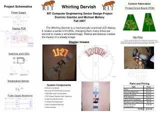
Motor. RPM Detect. Servo Board. Digital Controller – HCS12 Analog I/O to Motor Board Motor Speed In Next Speed Out Motor Accel Out Digital Inputs Position/Level Switch Sensors Hot Plate at Temp. No more wafers to process Wafer sender ready Wafer receiver cassette full

Photolithography Machine Control System RIT Computer Engineering Senior Design Project
E N D
Presentation Transcript
Motor RPM Detect Servo Board Digital Controller – HCS12 Analog I/O to Motor Board Motor Speed In Next Speed Out Motor Accel Out Digital Inputs Position/Level Switch Sensors Hot Plate at Temp. No more wafers to process Wafer sender ready Wafer receiver cassette full Wafer receiver ready Digital Outputs Store finished wafer Load next incoming wafer Solenoid Outputs Switch Sensors Hot Plate Entrance Wafer Cassette Holder Spin Chuck Vacuum Tube Bake Chuck Vacuum Tube Wafer Output Cartridge (25 wafers) Wafer Input Cartridge (25 wafers) Exit Wafer Cassette Holder Top Down View Solenoids HCS 12 LCD Panel HC11 SPI Interface Clk SDI/MISO SDO/MOSI Keypad ¾ Overhead View Cost Breakdown Photolithography Machine Control System RIT Computer Engineering Senior Design Project Ben Conrad February 13, 2004 Mark Edwards • How We Did It • Parts Used in System I/O Circuit • (1) HCS12 Microcontroller • (4) 74F675A 16-bit Serial In, Parallel Out Shift Registers • (2) 74F676 16-bit Parallel In, Serial Out Shift Registers • (2) LM741 Operational Amplifiers • (2) DAC0800 8-bit Digital to Analog Converters The Solitec Model 8360 spin casting and temperature controlled positive develop bake system is used in the photolithography process of making microelectronic circuits on silicon wafers. It automates the process of applying photoresist and baking a wafer, and is fully programmable through user input. This is accomplished through a keypad and LCD display. The user enters a series of operations with parameters on the keypad, thus forming “recipes” for the processing of particular sets of wafers. The main modules visible to the user are the digital display and input keypad, the input wafer cartridge, the chemical application spin chuck, the bake chuck, and the output wafer cartridge. The Team Technological Arts’ HSC12 Board Over 4000 lines of HCS12 assembly code was written to operate both the system and UI HCS12s. How It Works Coating the wafer with photoresist or developing it by wet etching off layers after masking is an essential step in the process of creating microchips. In either track, the control system loads a wafer from the input cartridge, then moves it to the spin chuck. Once on the spin chuck, a vacuum is applied. The spin chuck is then accelerated to anywhere from 0-8000RPM while various chemicals are applied to the wafer. The 8360 has the ability to dispense a main chemical (developer), de-ionized water, and an air stream of nitrogen. When finished, the system moves the wafer to the bake chuck, where the wafer is heated for a variable, user-defined length of time. Finally, the system moves the wafer to the output cartridge, and the wafer is ready to be processed by another system. The software controlled the inputs and outputs diagrammed (left) by expanding the HCS12’s input and output capabilities through the use of shift registers (below). Dual DAC’s provided analog signals which controlled the motor speed. The top-down diagram shows the wafer input and wafer output cartridges located on opposite ends of the line while the spin chuck and bake chuck are in the center. Vacuum tubes hold the wafers onto each chuck as they are processed. The gray rectangle represents a tray which is able to move between the input and output cartridge for wafer loading and unloading, respectively. The 3/4th overhead view diagram shows the holes cut into the system tray to allow each chuck to move up or down to allow the tray to move to one of its three positions (at input, center, at output.) Conveyer belts move the wafer from the input assembly and to the output assembly. The black squares represent three switches used for position sensing on the system tray and two vacuum sensors on the vacuum tubes to determine if a wafer is currently making contact with the tube (and thus on the tube’s chuck.) Control System Block Diagram Solitec 8360 in RIT’s Fab User Interface • Design Goals • Meet customer requirements – system able to hold 10 “recipes” for wafer processing, control wafer speed from 0-8000RPM, timing accurate to 0.1 seconds. • Allow use on coat and develop tracks – provide recipes general enough for controller to function on either machine • Save RIT money – our total cost is $500 compared to $25,000 from industry – 98% savings • Future Expandability • - Software handles extra sensors which may be added later • - System I/O hardware provides twice the I/O needed allowing expansion to machine with more processing stations Standby Mode • Seven Executable Commands • DEV#1: Dispense developer solution • PREWET: Dispense de-ionized(DI) water • RINSE: Dispenses DI water to clean wafer • N2: Dispenses Stream of Nitrogen (N2) • SPIN: Spin Dry the wafer • WAIT: Static delay option. • END PGM: End the program • Parameters • Time: .1 – 999.9 sec. (.1 second resolution) • Speed: 0-7,999 RPM Run Mode System I/O Hardware Program Mode UI Controller Status Mode A collaborative effort between RIT Computer Engineering and Microelectronic Engineering Special thanks to: John C. Nash, Dr. Alan D. Raisanen, Thomas J. Grimsley, and Dr. Roy Czernikowski